AI technical title is built by Patsnap AI team. It summarizes the technical point description of the patent document.
a non-volatile, semiconductor technology, applied in static storage, digital storage, instruments, etc., can solve the problems of increasing the number of data units, consuming a lot of power, and taking a long time to load data for each increase in data units, etc., to achieve the effect of large storage capacity
Inactive Publication Date: 2005-08-30
KIOXIA CORP
View PDF15 Cites 149 Cited by
Summary
Abstract
Description
Claims
Application Information
AI Technical Summary
This helps you quickly interpret patents by identifying the three key elements:
Problems solved by technology
Method used
Benefits of technology
Benefits of technology
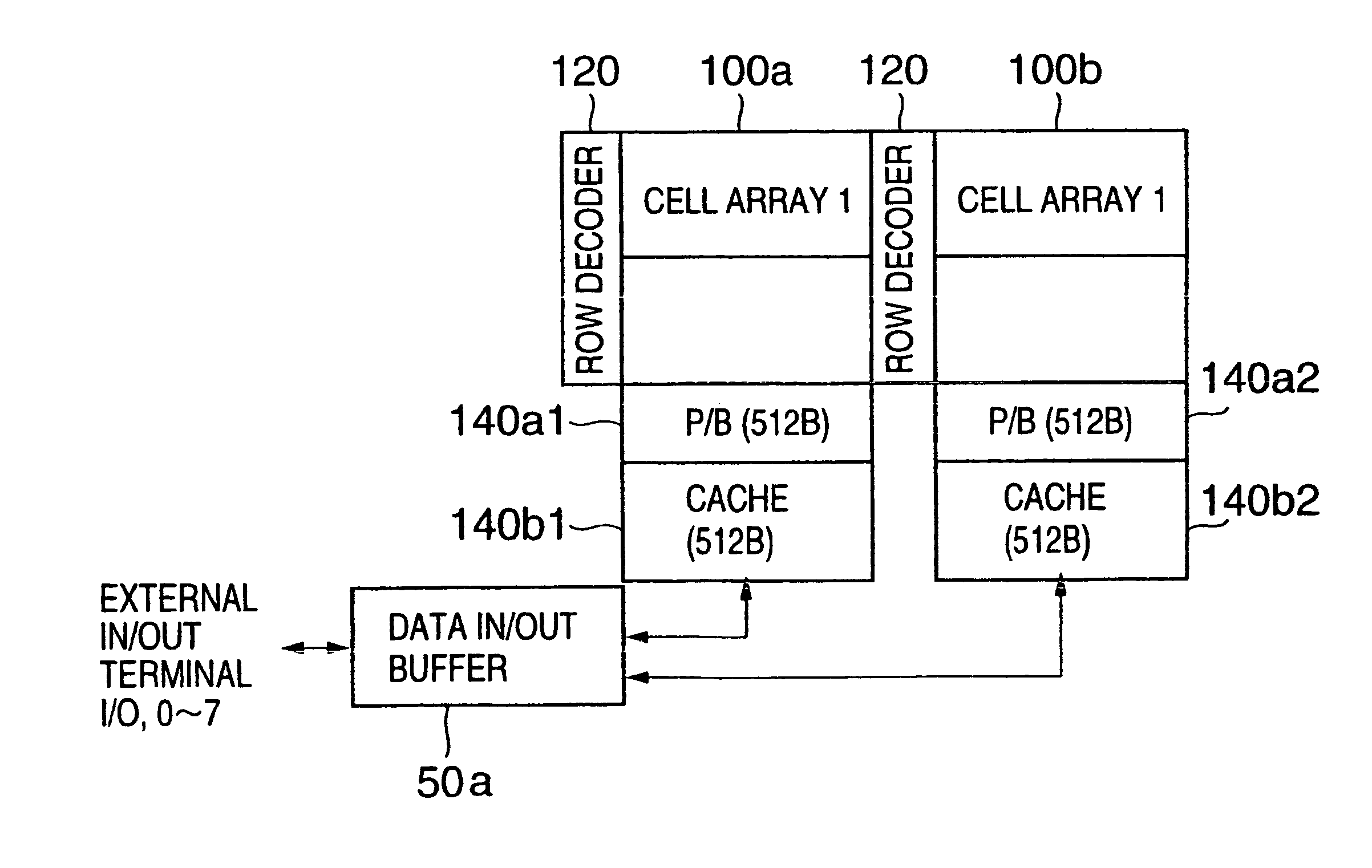
[0029]A purpose of the present invention is to provide a non-volatile semiconductor apparatus having a multilevel function for large storage capacity and a caching function for high-speed data load time.
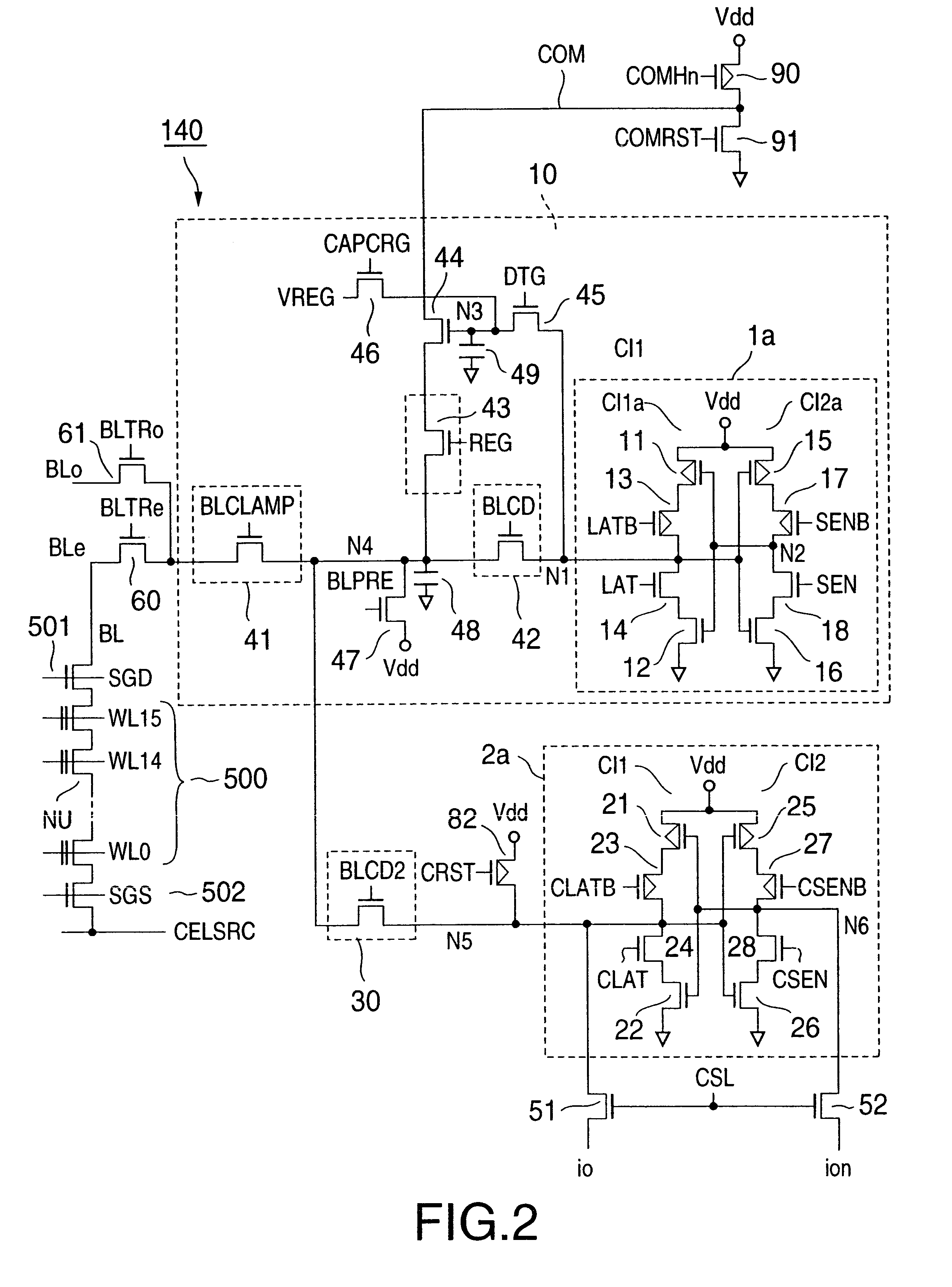
[0042]The cooperation of the first and the second latches offers a high-speed EEPROM having a caching function.
[0046]The boosting capacitor controls the potential at the sense node while data on a bit line is being sensed, thus precisely adjusting two-level data “HIGH” and “LOW” retrieved at the sense node with respect to the threshold level of the sense amplifier for attaining wide margin of sensing.
[0048]These sequential sensing operations with potential boosting achieve accurate data judgement with no relation to variation in sense amplifier-threshold level by lowering data level “LOW” retrieved at the sense if it is not sufficiently low due to high turn-on resistance of a selected memory cell. Furthermore, lowering a retrieval voltage at the clamp transistor after data transfer prevents the potential at the sense node from going to a negative level, as a result of potential boosting, for retrieving originally sufficiently low level “LOW”.
Problems solved by technology
Increase in the number of cell array division, however, takes a long time to load data for each increase in data unit to be programmed.
Moreover, increase in the number of cell array division requires a large chip and causes high consumption of power.
Enhancement in effective programming speed only by cell array division takes a long data load time in two-level operation thus inefficient.
Method used
Image
Click on the blue label to locate the original text in one second.
Reading with bidirectional positioning of images and text.
Examples
first embodiment
[0186]A multilevel logic operation in the first embodiment is disclosed in detail.
[0187]The first embodiment performs a multilevel logical operation under the relationship between a threshold level Vt of the memory cell 100 and 2-bit data, as illustrated in FIG. 43B.
[0188]The Vt-data relationship in FIG 43B is different from that in FIG. 43A. The same tact in FIGS. 43A and 43B is that the upper-bit data and the lower-bit data correspond to different row addresses. In detail, only in a multilevel operation, two addresses are prepared for the same cell to be selected.
[0189]Row addresses allocated to the upper and the lower bits are called the first row address for multilevel operation and a second row address for multilevel operation, respectively.
[0190]In FIG. 43B, the first (upper) bit and the second (lower) bit are the data in selection of the first row address and the second row address for multilevel operation, respectively. For example, the data ““10” is composed of the first (u...
second embodiment
[0328]To overcome such a problem, the second embodiment performs resetting of the second latch 2a just after data transfer from the latch 2a to the first latch 1a, as shown in FIG. 26, or performs the resetting always before programming operation.
[0329]The resetting of the second latch 2a is required before the initial data loading. However, resetting at unstable timing to the latch 2a during programming can be eliminated with no resetting at entry of “80H” and address daring programming.
[0330]FIG. 27 illustrates a programming operation using a cache memory for eliminating such resetting at unstable timing, which is applicable to the operations FIGS. 25A to 25C.
[0331]In detail, 2-page simultaneous programming starts after 2-page data loading “Load 1” and “Load 2”, and then, on completion of data transfer from the second latch 2a to the first latch la and latch (2a)-resetting (C, Rst), R / BB is set a quasi-ready state “HIGH”.
[0332]This sequence allows resetting the latch 2a only befor...
third embodiment
[0343]The third embodiment thus also achieves high effective programming speed although programming in the multilevel made takes long compared to usual two-level mode for storing 1-bit data to one nonvolatile memory cell.
PUM
Abstract
A non-volatile semiconductor device has a memory cell array having electrically erasable programmable non-volatile memory cells, reprogramming and retrieval circuits that temporarily store data to be programmed in the memory cell array and sense data retrieved from the memory cell array. Each reprogramming and retrieval circuit has a first latch and a second latch that are selectively connected to the memory cell array and transfer data each other. A controller controls the reprogramming and retrieval circuits on data-reprogramming operation to and data-retrieval operation from the memory cell array. Each reprogramming and retrieval circuit has a multilevel logical operation mode and a caching operation mode. In the multilevel logical operation mode, re-programming and retrieval of upper and lower bits of two-bit four-level data is performed using the first and the second latches in storing the two-bit four-level data in one of the memory cells in a predetermined threshold level range. In the caching operation mode, data transfer between one of the memory cells selected in accordance with a first address and the first latch is performed while data transfer is performed between the second latch and input / output terminals in accordance with a second address with respect to one-bit two-level data to be stored in one of the memory cells.
Description
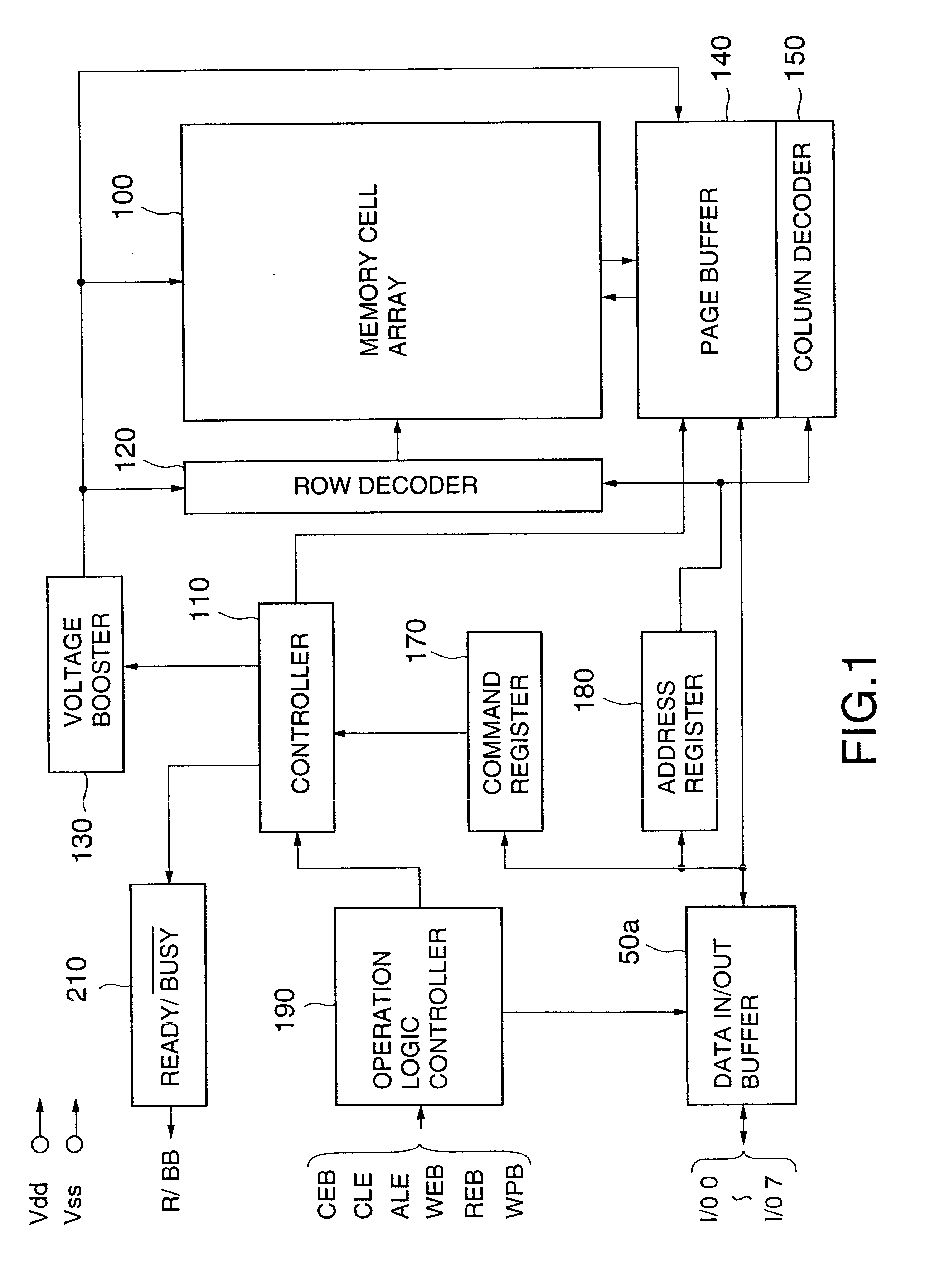
CROSS REFERENCE TO RELATED APPLICATIONS[0001]This application claims benefit of priority under 35 USC §119 to Japanese Patent Applications Nos. 2000-63798 and 2000-323199 filed on Mar. 8, 2000 and Oct. 23, 2000, respectively, in Japan, the entire contents of which are incorporated by reference herein.BACKGROUND OF THE INVENTION[0002]The present invention relates to an electrically erasable programmable read-only memory (EEPROM). Particularly, this invention relates to a data-reprogramming / retrieval circuit that temporally stores data to be programmed or data to be retrieved for a caching function or a multilevel logical function.[0003]Focused on in the semiconductor industry is reduction of cost per bit for high-capacity flash EEPROMs used as a file memory by miniaturization of cell structure with process techniques and also by multilevel logic techniques for high capacity.[0004]FIG. 42 is a circuit block diagram of a data-reprogramming / retrieval circuit (called a page buffer herein...
Claims
Application Information
Patent Timeline
Application Date:The date an application was filed.
Publication Date:The date a patent or application was officially published.
First Publication Date:The earliest publication date of a patent with the same application number.
Issue Date:Publication date of the patent grant document.
PCT Entry Date:The Entry date of PCT National Phase.
Estimated Expiry Date:The statutory expiry date of a patent right according to the Patent Law, and it is the longest term of protection that the patent right can achieve without the termination of the patent right due to other reasons(Term extension factor has been taken into account ).
Invalid Date:Actual expiry date is based on effective date or publication date of legal transaction data of invalid patent.

