3D (three-dimensional) NAND memory and manufacturing method thereof

A manufacturing method and memory technology, applied in the field of semiconductors, can solve the problems of difficult through-holes, long signal transmission paths, unstable signal transmission, etc., and achieve the effects of reducing parasitic parameters, strengthening control capabilities, and increasing cut-off frequency

Active Publication Date: 2014-03-26
SEMICON MFG INT (SHANGHAI) CORP
View PDF13 Cites 46 Cited by
  • Summary
  • Abstract
  • Description
  • Claims
  • Application Information

AI Technical Summary

Problems solved by technology

Moreover, for the lower-level storage unit, the signal transmission path will be relatively long, which will easily lead to unstable signal transmission
Moreover, for memory cells with a large number of layers, it is very difficult to make through holes with different depths in the same process.

Method used


Image

  • 3D (three-dimensional) NAND memory and manufacturing method thereof
  • 3D (three-dimensional) NAND memory and manufacturing method thereof
  • 3D (three-dimensional) NAND memory and manufacturing method thereof

Examples


Embodiment Construction

[0045] In order to make the above objects, features and advantages of the present invention more comprehensible, specific implementations of the present invention will be described in detail below in conjunction with the accompanying drawings.

[0046] In the following description, numerous specific details are set forth in order to provide a thorough understanding of the present invention. However, the present invention can be implemented in many other ways different from those described here, and those skilled in the art can make similar extensions without violating the connotation of the present invention, so the present invention is not limited by the specific implementations disclosed below.

[0047] Circuit structure of 3D NAND memory

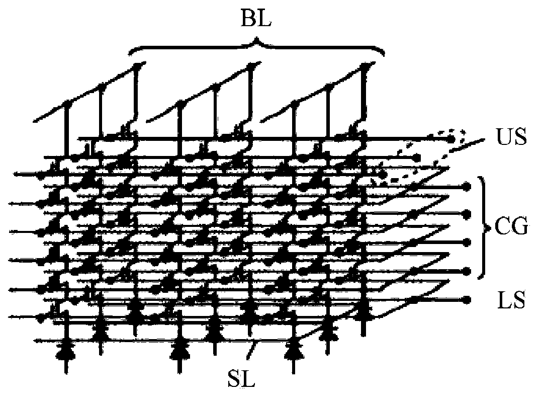
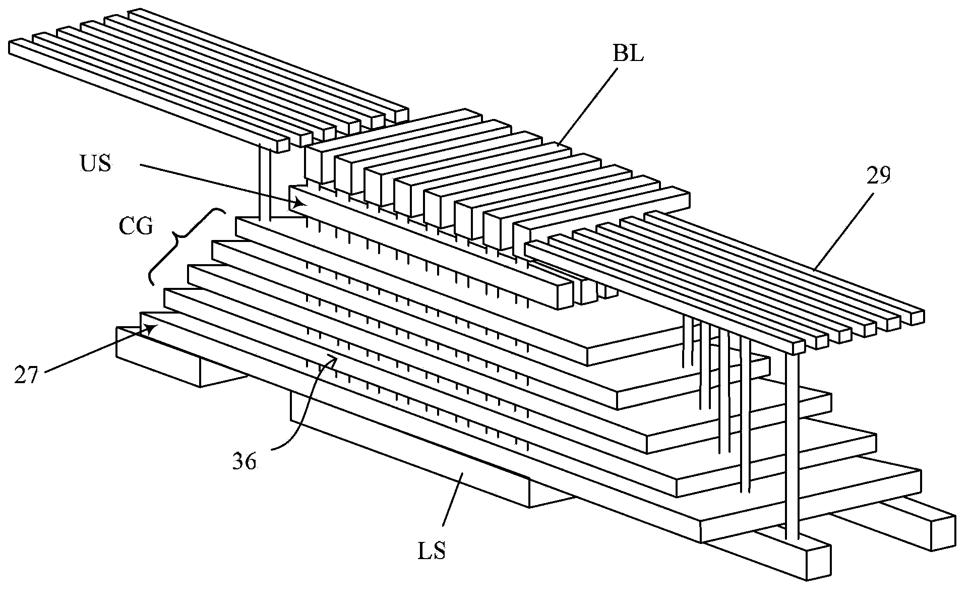
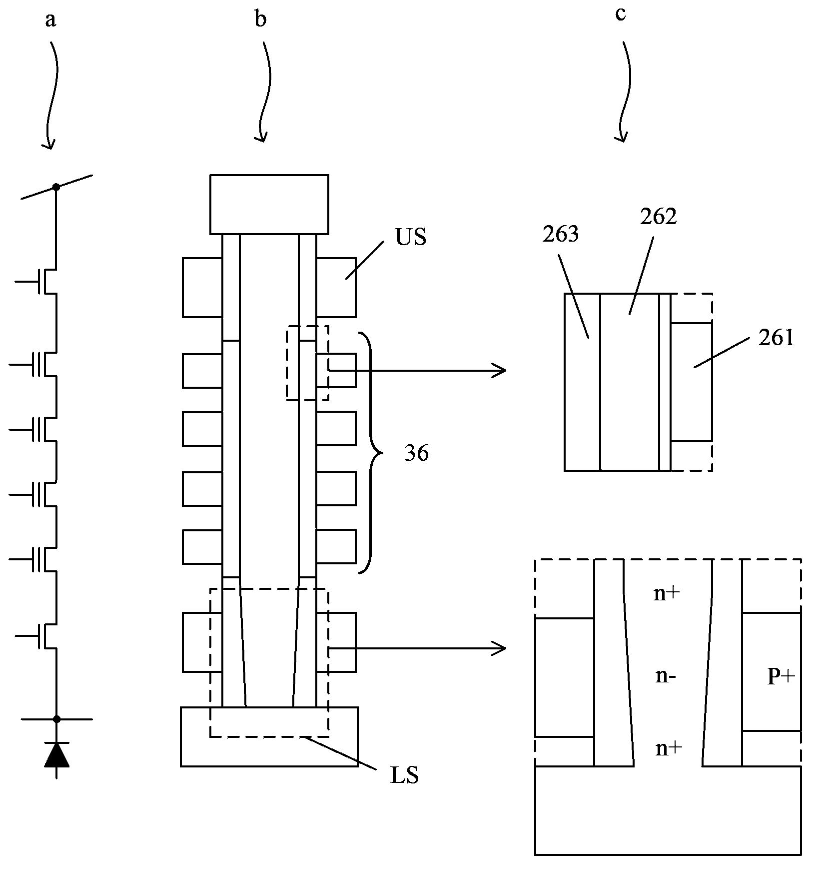
[0048] Such as Figure 7 Shown is a schematic circuit diagram of an embodiment of the 3D NAND memory of the present invention. The 3D NAND memory of the present invention retains the original memory array (Memory anay) of the 3D NAND ...


PUM


Abstract

The invention discloses a 3D (three-dimensional) NAND memory and a manufacturing method of the 3D NAND memory. The 3D NAND memory comprises multiple layers of storage arrays and multiple layers of control grid circuits, wherein each layer of the control grid circuit is electrically connected to the same layer of the storage array, so that selection of each layer of the storage array is realized; each layer of the control grid circuit is obtained by cascading a same number of transistors; grids of all the transistors of the control grid circuits are electrically connected to control wires; the number of the control wires is as the same as that of the transistors comprised in each layer of the control grid circuit; the grids of different transistors positioned on the same layer of the control grid circuit are electrically connected to different control wires. According to the 3D NAND memory, a small number of input control wires SSL select a large number of control grid layers through the control grid circuits, so that the area and the volume of the whole memory cannot be enlarged due to the increase of the number of the required layers of control grids when the storage capacity of the memory is improved due to the increase of the number of storage unit layers.

Description

technical field [0001] The invention relates to the field of semiconductors, in particular to a 3D NAND memory and a manufacturing method. Background technique [0002] With the industry's demand for memory with high integration density and large storage capacity, 3D NAND (three-dimensional NAND) memory has emerged as the times require. A 3D NAND structure such as Figure 1 to Figure 6 shown. in, figure 1 It is a circuit schematic diagram of 3D NAND, which includes word line BL (Bit Line), top selection gate US (Upper SG), control gate CG (Control Gate), bottom selection gate LS (Lower SG), source line SL (Source Line ). The current is unidirectionally output from the memory array by the source line SL (Source Line). The selection signal of the word line BL (Bit Line), the selection signal common to the top selection gate US (Upper SG) and the bottom selection gate LS (Lower SG), and the selection signal of the control gate CG (Control Gate) respectively from the three-...

Claims


Application Information

Patent Timeline
Patent Type & Authority Applications(China)
IPC IPC(8): G11C16/06H01L27/115H01L21/8247
Inventor 何其旸
Owner SEMICON MFG INT (SHANGHAI) CORP
Why Eureka
Try Eureka