
Ultra thin body fully-depleted SOI mosfets

Inactive Publication Date: 2006-01-05
GLOBALFOUNDRIES INC
View PDF35 Cites 59 Cited by
  • Summary
  • Abstract
  • Description
  • Claims
  • Application Information

AI Technical Summary

Benefits of technology

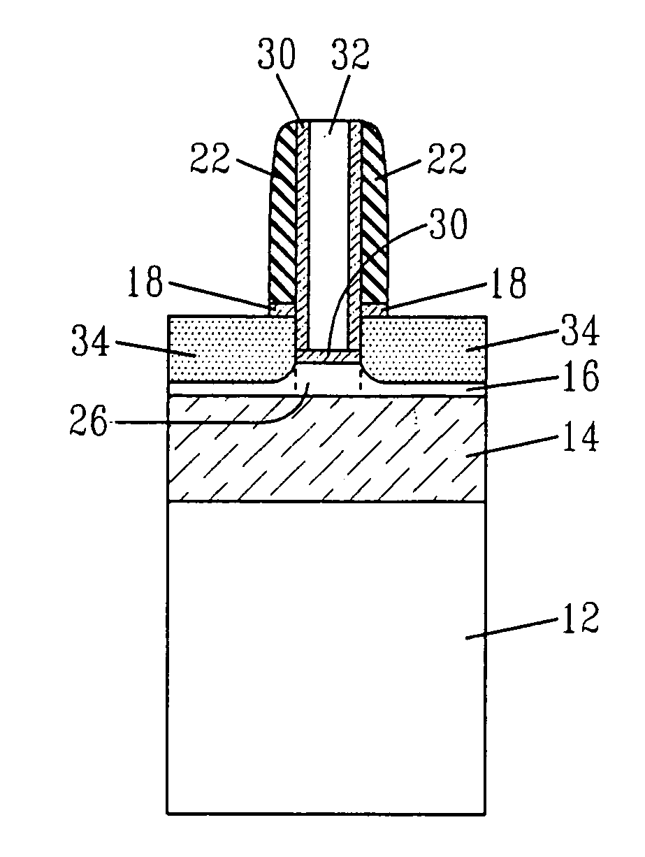
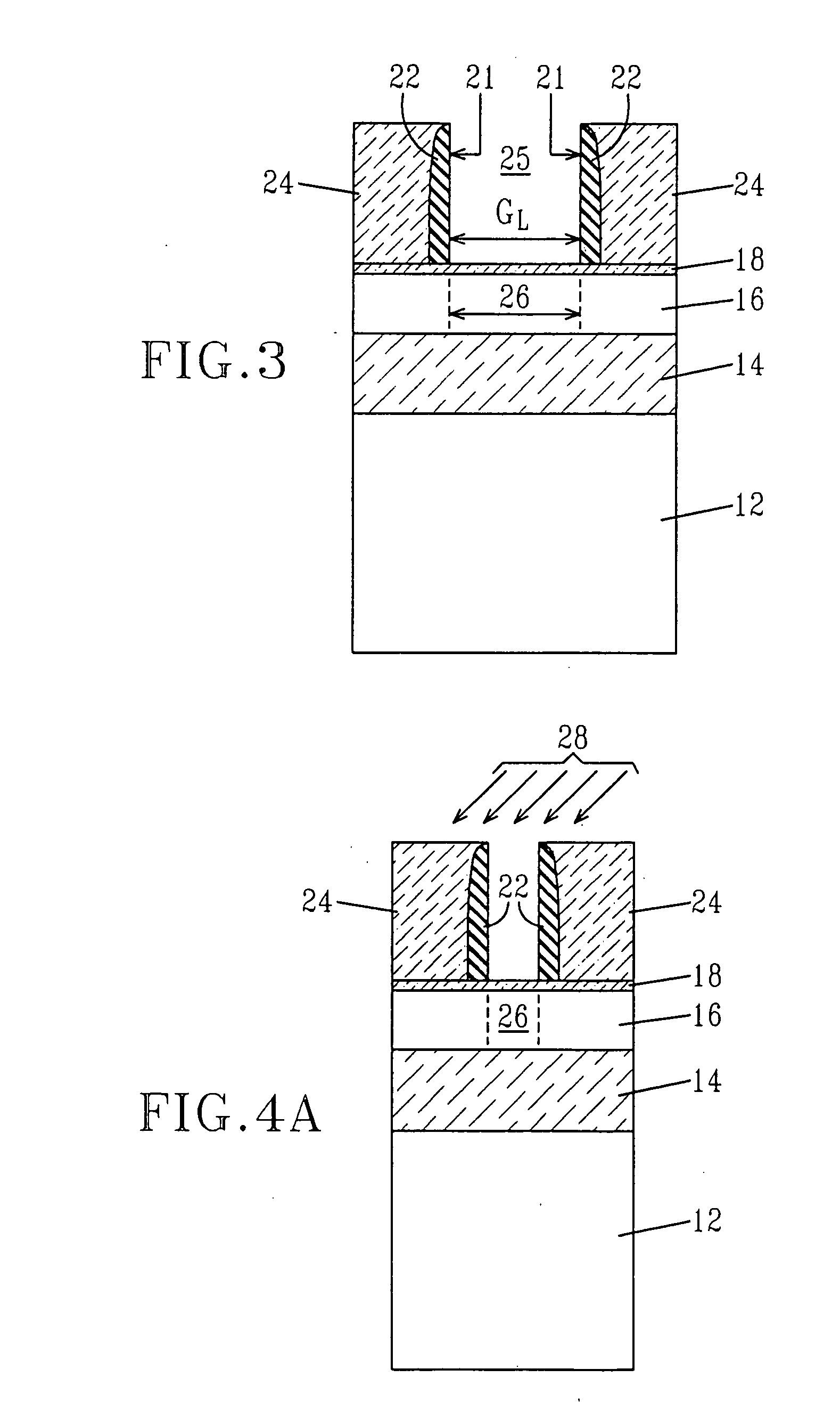
[0009] The present invention provides a method of creating ultra thin body fully-depleted SOI MOSFETs in which the SOI thickness changes with gate-length variations thereby minimizing the threshold voltage variations that are typically caused by SOI thickness and gate-length variations. This object is achieved in the present invention by using a replacement gate process in which nitrogen (or fluorine) is implanted to selectively retard (enhance) oxidation during formation of a recessed channel. A self-limited chemical oxide removal (COR) processing step can be used to improve the control in the recessed channel step.

Problems solved by technology

It is also known that fully-depleted SOI MOSFET devices with doped channels typically have very large threshold voltage variations.
This prior art method however cannot be extended any further because 1) the junction leakage current could be to high with high halo doping concentration; and 2) the doping fluctuation effect could dominate the threshold variations in narrow width devices.

Method used


Image

  • Ultra thin body fully-depleted SOI mosfets
  • Ultra thin body fully-depleted SOI mosfets
  • Ultra thin body fully-depleted SOI mosfets

Examples


Embodiment Construction

[0030] The present invention, which provides a method for threshold voltage variations control in ultra thin fully-depleted SOI MOSFETS, will now be described in greater detail by referring to the drawings that accompany the present application.

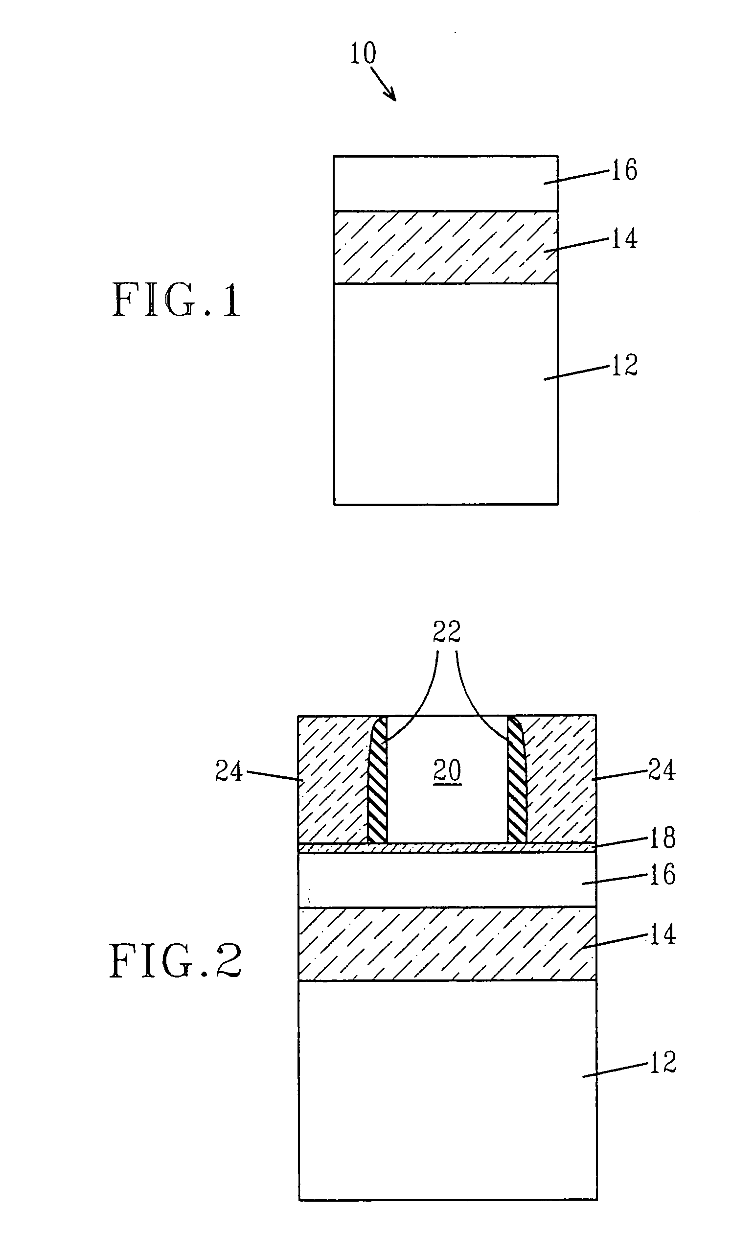
[0031] Referring to FIG. 1 there is shown an initial SOI substrate 10 that can be employed in the present invention. The initial SOI substrate 10 includes a bottom Si-containing layer 12, a buried insulating layer 14, such as an oxide or nitride, located on the bottom Si-containing layer 12, and a top Si-containing layer 16, i.e., the SOI layer, located on the buried insulating layer 14. The term “Si-containing layer” denotes any material that includes silicon. Illustrative examples of Si-containing materials include, but are not limited to: Si, SiGe, SiGeC, SiC, polysilicon, i.e., polySi, epitaxial silicon, i.e., epi Si, amorphous silicon, i.e., a:Si, and multilayers thereof. Typically, layers 12 and 16 of the SOI substrate 10 are both comp...


PUM


Abstract

A method of creating ultra tin body fully-depleted SOI MOSFETs in which the SOI thickness changes with gate-length variations thereby minimizing the threshold voltage variations that are typically caused by SOI thickness and gate-length variations is provided. The method of present invention uses a replacement gate process in which nitrogen is implanted to selectively retard oxidation during formation of a recessed channel. A self-limited chemical oxide removal (COR) processing step can be used to improve the control in the recessed channel step. If the channel is doped, the inventive method is designed such that the thickness of the SOI layer is increased with shorter channel length. If the channel is undoped or counter-doped, the inventive method is designed such that the thickness of the SOI layer is decreased with shorter channel length.

Description

BACKGROUND OF INVENTION [0001] The present invention relates to semiconductor integrated circuit devices as well as their fabrication, and more particularly to ultra thin body, e.g., channel, fully-depleted silicon-on-insulator (SOI) metal oxide semiconductor field effect transistor (MOSFET) devices in which the threshold voltage variation of each device is controlled. [0002] In semiconductor processing, silicon-on-insulator (SOI) technology is becoming increasingly important since it permits the formation of high-speed integrated circuits. In SOI technology, a buried insulating layer, especially a buried oxide, electrically isolates a top Si-containing layer from a bottom Si-containing substrate layer. The top Si-containing layer, which is oftentimes referred to in the art as the SOI layer, is generally the area in which active devices such as transistors are formed. Devices formed using SOI technology offer many advantages over the bulk counterparts including, for example, higher ...

Claims


Application Information

Patent Timeline
IPC IPC(8): H01L29/76H01L21/00
CPCH01L29/66545H01L29/78696H01L29/66772
Inventor DORIS, BRUCE B.IEONG, MEIKEIREN, ZHIBINSOLOMON, PAUL M.YANG, MIN
Owner GLOBALFOUNDRIES INC
Learn More