Circuit board testing jig

a circuit board and testing jig technology, applied in electrical testing, measurement devices, instruments, etc., can solve the problems of easy damage of the jig, more time spent by the operator performing the testing process, etc., and achieve the effect of quick and easy setup of the circuit board testing jig and saving setup tim

Inactive Publication Date: 2005-09-20
PEGATRON
View PDF2 Cites 2 Cited by
  • Summary
  • Abstract
  • Description
  • Claims
  • Application Information

AI Technical Summary

Benefits of technology

[0018]In view of the foregoing, this invention is to provide a circuit board testing jig, which can assemble and aligns a circuit board easily.
[0020]As mentioned above, regarding to the circuit board testing jig of the invention, the edge of the carrier alignment hole adjacent to the second surface is formed with a guiding angle. Therefore, the invention can quickly and easily setup the circuit board testing jig to save setup time and to protect the testing jig.

Problems solved by technology

Thus, the operator may spend more time to perform this testing process.2. Jig is easily damaged: Referring to FIGS. 4 and 5, the pressure plate 11 of the circuit board testing machine 1 applies a force to the circuit board testing jig 2.

Method used


Image

  • Circuit board testing jig
  • Circuit board testing jig
  • Circuit board testing jig

Examples


Embodiment Construction

[0029]The circuit board testing jig according to preferred embodiments of the invention will be described herein below with reference to the accompanying drawings, wherein the same reference numbers refer to the same elements.

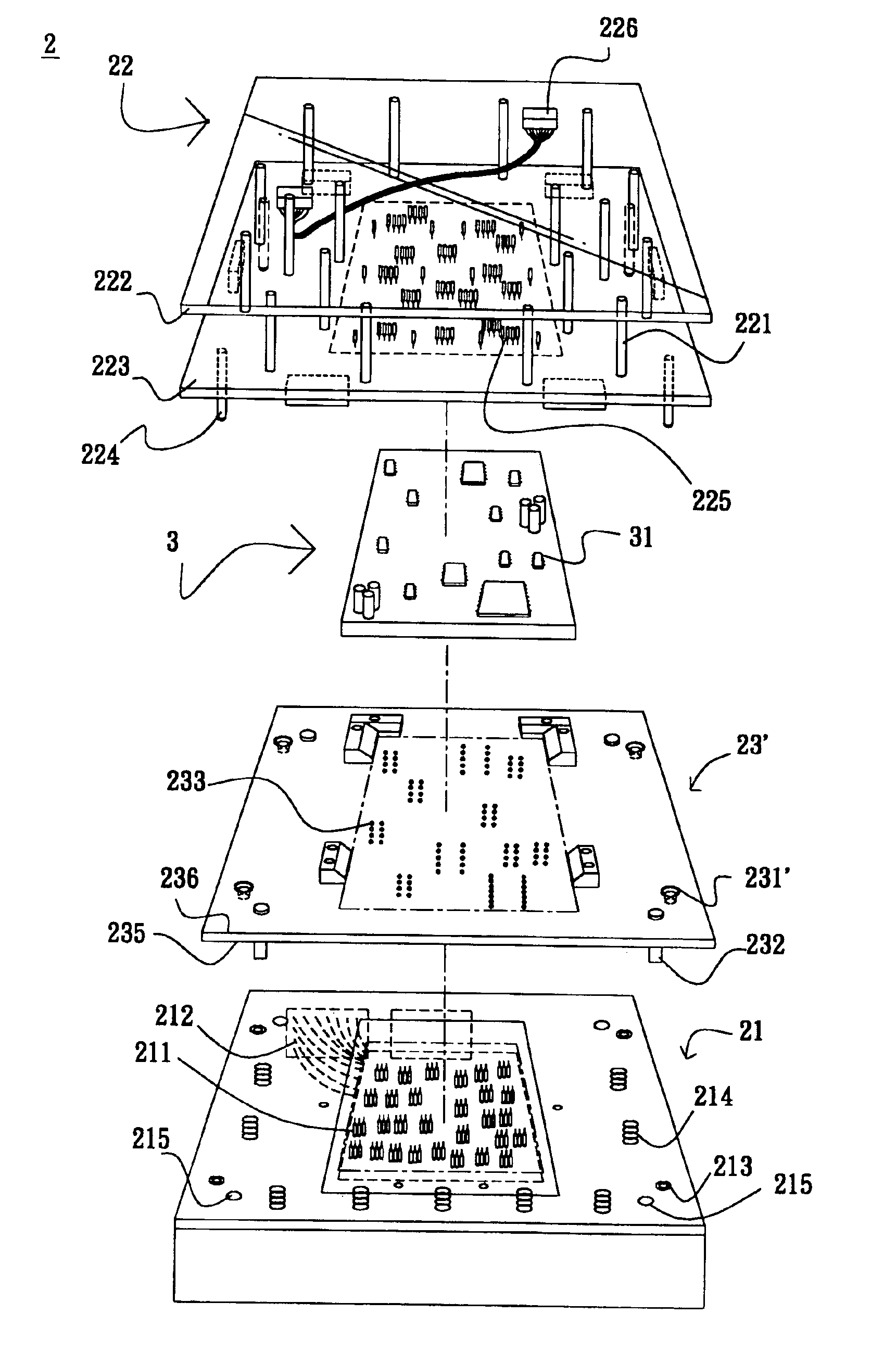
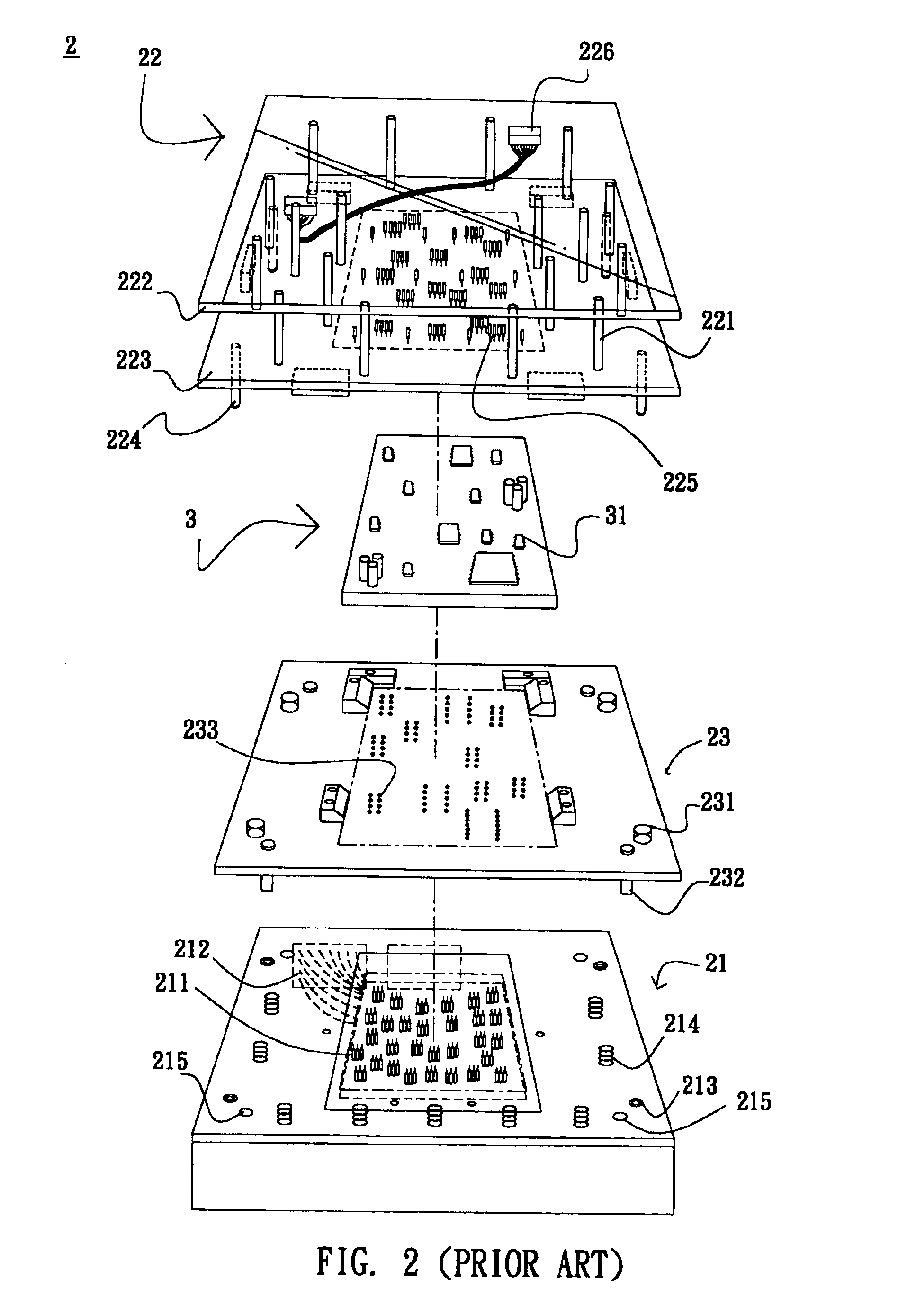
[0030]Referring to FIG. 6, the circuit board testing jig 2 comprises a first testing unit 21, a second testing unit 22 and a carrier 23′. In the embodiment, the first testing unit 21 and second testing unit 22 are the same as the previous-mentioned first testing unit 21 and the second testing unit 22 (as shown in FIG. 2).

[0031]Referring to FIG. 6, the carrier 23′ has a first surface 235 and a second surface 236.

[0032]The carrier 23′ has at least one carrier alignment hole 231′ corresponding to the first alignment hole 213 of the first testing unit 21. The carrier alignment hole 231′ is set through the first surface 235 and the second surface 236. The diameter of the section of the carrier alignment hole 231′ adjacent to the second surface 236 is larger than the...


PUM


Abstract

A circuit board testing jig tests a circuit board. The jig includes a first testing unit, a second testing unit, and a carrier. The first testing unit has at least one first alignment hole. The second testing unit has at least one first alignment rod. The carrier is set between the first testing unit and the second testing unit. The carrier includes a first surface, a second surface, and at least one carrier alignment hole. The first surface of the carrier faces the first testing unit. The second surface of the carrier carries the circuit board and faces the second testing unit. The carrier alignment hole passes through the first surface of the carrier to the second surface of the carrier. The edge of carrier alignment hole on the second surface has a guiding angle. The first alignment rod passes through the carrier alignment hole and then inserts into the first alignment hole.

Description

[0001]This Nonprovisional application claims priority under 35 U.S.C. § 119(a) on Patent Application No(s). 093100483 filed in Taiwan, Republic of China on Jan. 8, 2004, the entire contents of which are hereby incorporated by reference.BACKGROUND OF THE INVENTION[0002]1. Field of Invention[0003]The invention relates to a testing jig and, in particular, to a circuit board testing jig, which assembles and aligns the circuit board easily.[0004]2. Related Art[0005]For maintaining the fabrication quality of a circuit board, an electrical test for the circuit board or components of the circuit board is usually performed after the circuit board is manufactured.[0006]FIG. 1 is a schematic view showing a conventional circuit board testing equipment. The conventional circuit board testing equipment comprises a circuit board testing machine 1 and a circuit board testing jig 2 used in the circuit board testing machine 1.[0007]Referring to FIG. 1, the circuit board testing jig 2 comprises a firs...

Claims


Application Information

Patent Timeline
Patent Type & Authority Patents(United States)
IPC IPC(8): G01R1/04G01R1/02
CPCG01R1/0408
Inventor LEE, CHUNG-SHANLI, YUAN-CHIANGHSU, CHIH-KAI
Owner PEGATRON
Why Eureka
Try Eureka