

Dielectric antenna
a technology of dielectric antennas and antennas, applied in the direction of resonant antennas, elongated active elements, protecting materials, etc., can solve the problems of difficult to reduce the size, the efficiency of the antenna is extremely low, and the impedance to the miniaturization of wireless communication devices
- Summary
- Abstract
- Description
- Claims
- Application Information
AI Technical Summary
Benefits of technology
Problems solved by technology
Method used
Image

Examples
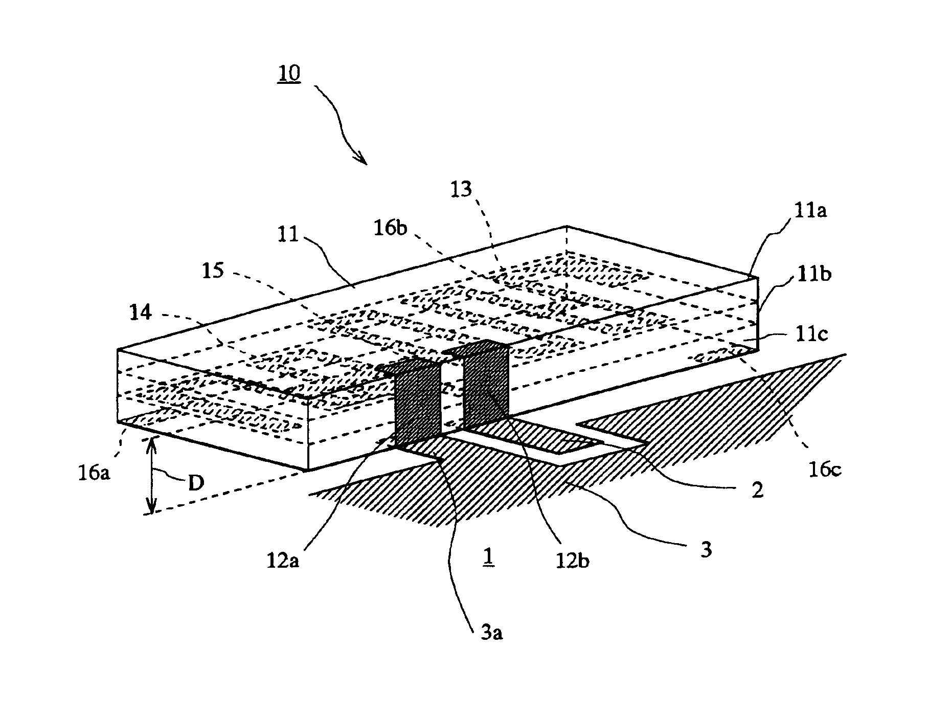
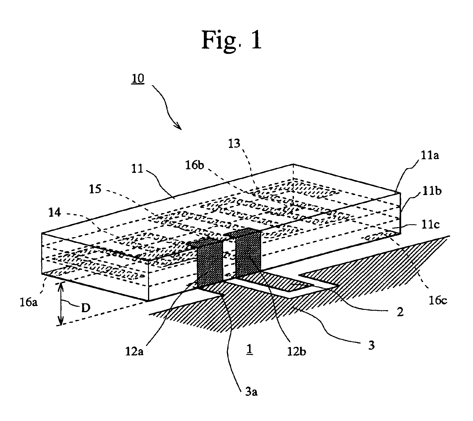
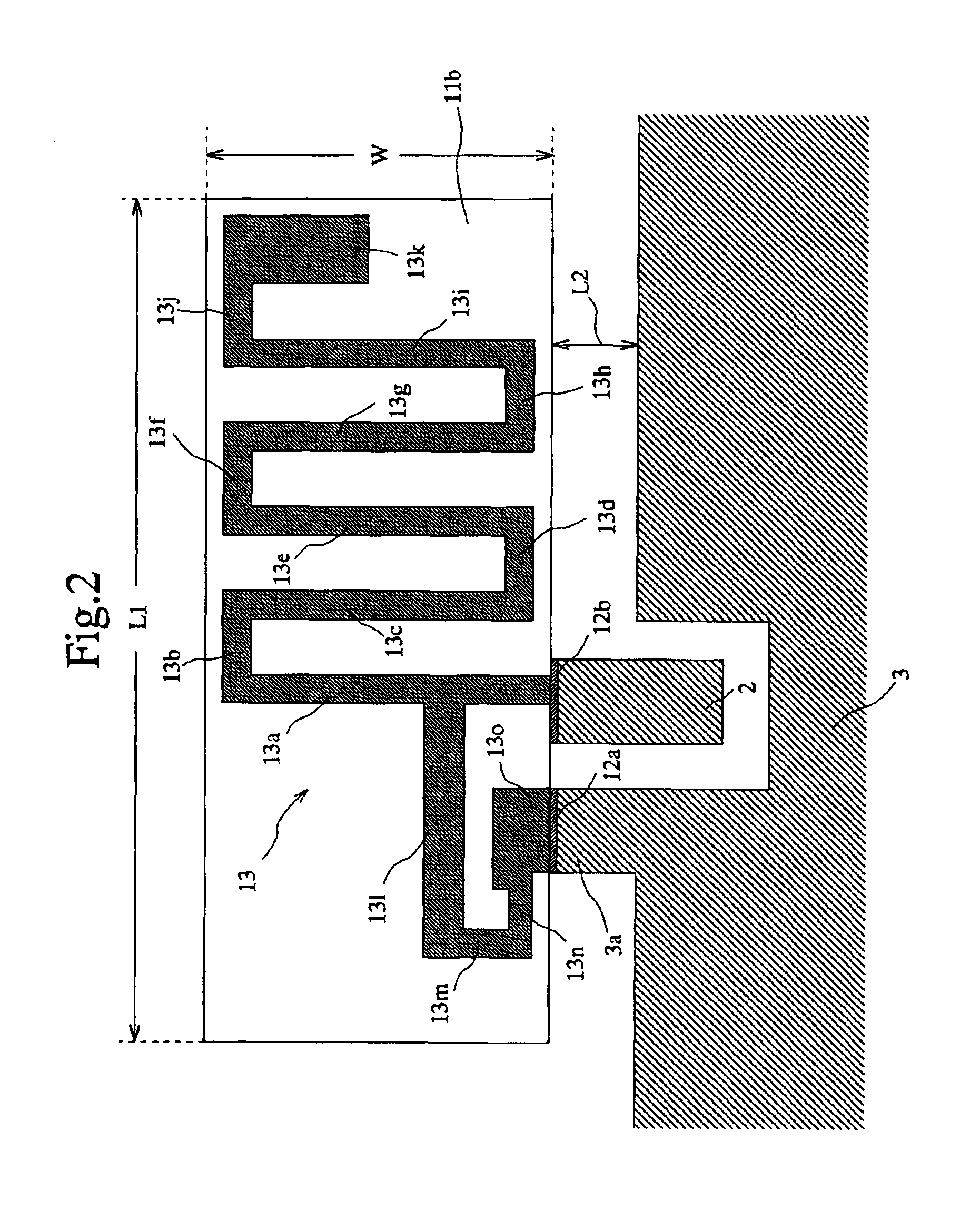
first embodiment
[0068]The VSWR characteristic shown in FIG. 13 was obtained when the dielectric antenna was mounted on the circuit board 1 by being spaced apart from the grounding conductor 3 on the circuit board 1 by the distance L2 (1 mm). In the case where the open stub 15 does not exist, small VSWR values are exhibited, that is, the VSWR is 3 or less at 2.22 to 2.84 GHz, 1.5 at 2.34 GHz, and 1.0 at 2.67 GHz. However, as a result of removal of the open stub 15, the resonance frequency is increased wholly by about 150 MHz. That is, to set the same resonance frequency as that in the first embodiment, it is necessary to increase the size of the antenna element by an amount for 150 MHz (about 6%) and to use a configuration for a larger size.
[0069]In the dielectric antenna 10 of the first embodiment, the open stub 15 is provided to enable control of the impedance including the state of coupling as well as adjustment of the resonance frequency. Thus, an effect other than the effect of achieving the 6%...
second embodiment
[0072]A dielectric antenna in the present invention will next be described.
[0073]As the second embodiment, a dielectric antenna for W-CDMA in the 2 GHz band was configured. FIG. 14 is a perspective see-through view of the dielectric antenna in the second embodiment of the present invention, FIG. 15 is a plan view of a first antenna element, and FIG. 16 is a plan view of a second antenna element.
[0074]Referring to the drawings, the dielectric antenna 20 has a laminated member 21 laminated from flat substrates 21a, 21b, and 21c (hereinafter referred to simply as “substrate”) having an insulating property and made of a dielectric ceramic material. External terminals 22a and 22b are provided on one side surface of the laminated member 21.
[0075]Conductors which form the first antenna element (hereinafter referred to simply as “antenna element”) 23 are provided on an upper surface of the intermediate layer substrate 21b. Also, conductors which form the second antenna element (hereinafter ...
third embodiment
[0089]A dielectric antenna in the present invention will next be described.
[0090]An example of a 2.4 GHz band dielectric antenna presently used for mobile communication will be described as the third embodiment, as is that described as the first embodiment. In the third embodiment, the same open stub as that described above is provided and an end portion of antenna is branched to enable further miniaturization in comparison with first embodiment.
[0091]FIG. 18 is a perspective see-through view of the dielectric antenna in the third embodiment of the present invention, FIG. 19 is a plan view of a first antenna element, and FIG. 20 is a plan view of a second antenna element.
[0092]Referring to these drawings, the dielectric antenna 30 has a laminated member 31 laminated from flat substrates 31a, 31b, and 31c (hereinafter referred to simply as “substrate”) having an insulating property and made of a dielectric ceramic material. External terminals 32a and 32b are provided on one side surf...
PUM
 Abstract
Description
Claims
Application Information