Radiation detecting apparatus and radiation imaging system

a radiation imaging system and detecting apparatus technology, applied in the field of radiation detecting apparatus and radiation imaging system, can solve the problems of insufficient cancellation accuracy of noise cancellation caused by offset components, insufficient noise cancellation of so-called dark outputs, and insufficient noise cancellation accuracy, so as to achieve good image and reduce noise

Inactive Publication Date: 2010-11-25
CANON KK
View PDF17 Cites 26 Cited by
  • Summary
  • Abstract
  • Description
  • Claims
  • Application Information

AI Technical Summary

Benefits of technology

[0017]According to the radiation detecting apparatus and the radiation imaging system of the present invention, noises can be decreased, and consequently a good image can be obtained.

Problems solved by technology

However, the cancellation of noises is insufficient by the compensation method of performing compensations only at the wiring crossing portions, which method is disclosed in US 2006 / 0065845 (Japanese Patent Application Laid-Open No. 2006-101394).
Moreover, the accuracy of the cancellation of the noises caused by offset components, the so-called dark outputs, is insufficient by the method disclosed in U.S. Pat. No. 6,696,687 (Japanese Patent Application Laid-Open No. 2001-56382), which method deducts the dark output of the dummy pixel arranged only at the end of the X-ray detection portion from the photo output of the whole X-ray detection portion.

Method used


Image

  • Radiation detecting apparatus and radiation imaging system
  • Radiation detecting apparatus and radiation imaging system
  • Radiation detecting apparatus and radiation imaging system

Examples


first embodiment

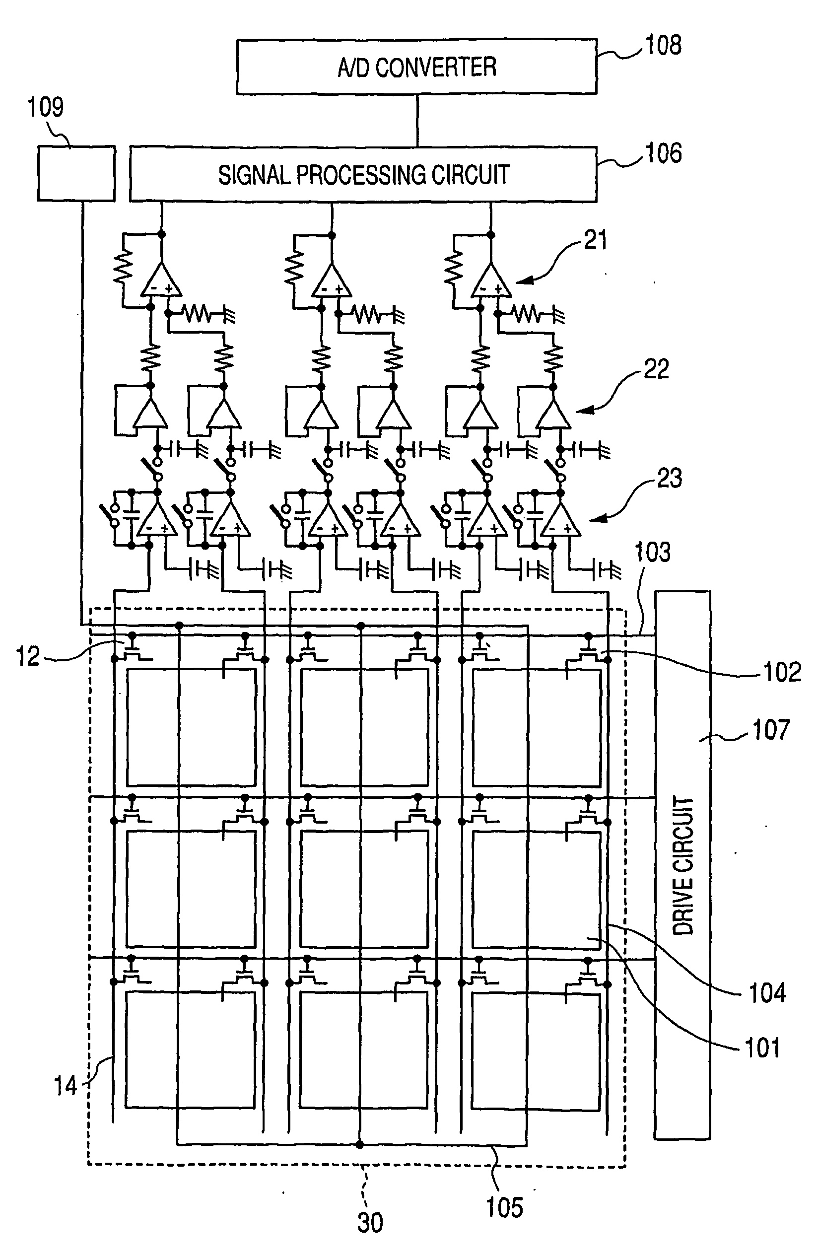
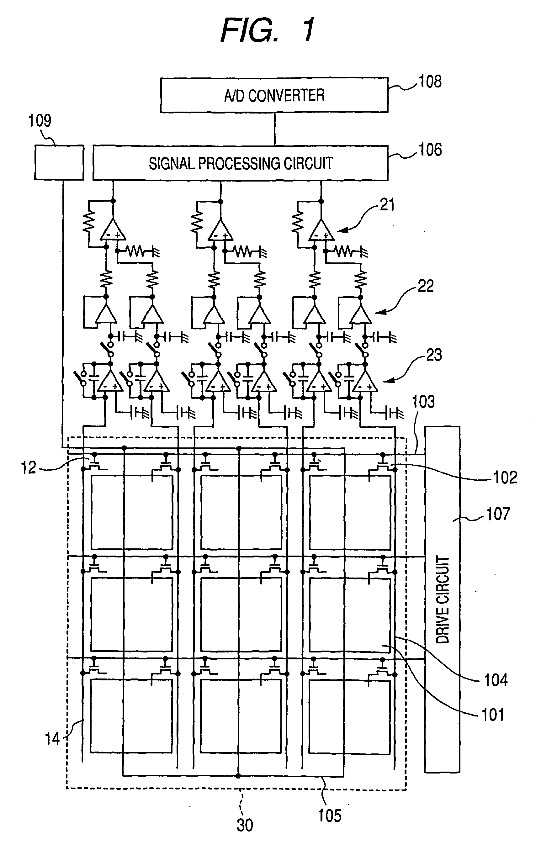
[0045]FIG. 1 is a schematic circuit diagram illustrating the configuration of a radiation detecting apparatus as a first embodiment of the present invention. In the present invention the radiation may be a visible light.

[0046]As illustrated in FIG. 1, the radiation detecting apparatus includes PIN type photoelectric conversion elements 101 as conversion elements for converting incident radiations into electric signals, and transfer TFTs 102 as first switch elements. Moreover, the radiation detecting apparatus includes drive lines 103 connected electrically to the gate electrodes of the transfer TFTs 102, and first signal lines 104 connected electrically to the source or drain electrodes as the main electrodes of the transfer TFTs 102. The transfer TFTs 102 include first main electrodes connected electrically to the first signal lines 104, second main electrodes connected electrically to the conversion elements 101, and gate electrodes, operating as control electrodes, connected elec...

second embodiment

[0077]FIG. 7 is a schematic circuit diagram illustrating the configuration of a radiation detecting apparatus as a second embodiment of the present invention. The present embodiment adopts a double gate structure in which each of the transfer TFTs 102 and the dummy TFTs 12 includes serially connected two TFTs, the gate electrodes of which are connected to one of the common drive lines 103. Then, as described below, the transfer TFTs 102 and the dummy TFTs 12 are polysilicon TFTs. By configuring the transfer TFTs 102 and the dummy TFTs 12 to have the double gate structures, the leak current of each of the TFTs 102 and 12 can be decreased, and consequently noises can be decreased to enable the obtainment of a good image.

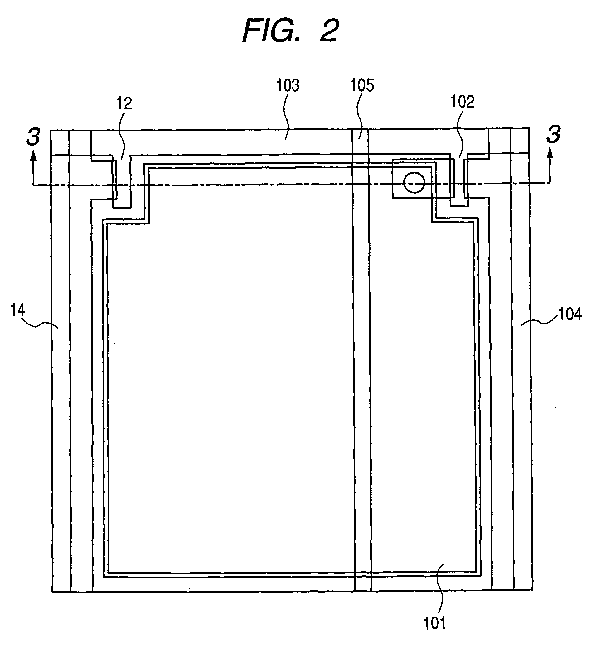
[0078]FIG. 8 is a schematic plan view of one pixel of a radiation detecting apparatus of the present embodiment. In FIG. 8, the reference numerals are same as those of FIG. 7. FIG. 9 is a schematic sectional view taken along a line 9-9 in FIG. 8.

[0079]As illustrated in...

third embodiment

[0082]FIG. 10 is a schematic circuit diagram illustrating the configuration of a radiation detecting apparatus as a second embodiment of the present invention.

[0083]As illustrated in FIG. 10, the radiation detecting apparatus includes a power source 501 capable of supplying bias potential and reference voltage wiring 502 for the dummy TFTs 12. The other components are denoted by the same signs as those in the preceding figures.

[0084]Also in the present embodiment, similarly to the first embodiment, the dummy signal lines 14 and the dummy TFTs 12 have the same layer configurations and the same sizes as those of the signal lines 104 and the transfer TFTs 102, respectively.

[0085]FIG. 11 is a schematic plan view of a pixel of the radiation detecting apparatus of the present embodiment. In FIG. 11, reference numerals are the same as those in FIG. 10. FIG. 12 is a schematic sectional view taken along a line 12-12 in FIG. 11.

[0086]A first electrode of the source and drain electrodes 304, w...


PUM


Abstract

A radiation detecting apparatus capable of obtaining good images including decreased noises includes a plurality of pixels, each having a photoelectric conversion element for converting an incident radiation into an electric signal and a a first switch element connected to the photoelectric conversion element and a second switch element being not connected to the conversion element; a first signal line; a second signal line; and a drive line, wherein the first switch element has a first main electrode connected electrically to the first signal line, a second main electrode connected electrically to the photoelectric conversion element, and a gate electrode connected electrically to the drive line, the second switch element has a first main electrode connected to the second signal line and a gate electrode connected electrically to the drive wiring common to the first switch element, and a differential means for outputting a signal corresponding to a difference between outputs from the first and second switch elements.

Description

TECHNICAL FIELD[0001]The present invention relates to a radiation detecting apparatus and a radiation imaging system. Incidentally, the present specification supposes that an electromagnetic wave, such as a visible light, an X ray, an α ray, a β ray, a γ ray, and the like, are also included in a radiation. And, a conversion element includes a photoelectric conversion element converting a light such as a visible light into an electric signal.BACKGROUND ART[0002]Conventionally, the radiography used for medical diagnostic imaging is classified into plain radiography for obtaining a still image, such as X-ray radiographing, and fluoroscopic radiography for obtaining a moving image. For each kind of radiography, the selection of the radiography is performed to include the selection of a radiographing apparatus as the occasion demands.[0003]In recent years, a flat-panel detector has been noticed, which includes a sensor panel on which pixels, each including a conversion element to convert...

Claims


Application Information

Patent Timeline
Patent Type & Authority Applications(United States)
IPC IPC(8): H01L27/146G01T1/208H04N5/32H04N5/335H04N5/357H04N5/361H04N5/365H04N5/369H04N5/374
CPCG01T1/2928H01L27/14609H01L27/14658H01L27/14663H04N5/378H04N5/32H04N5/357H04N5/3696H04N5/37457H01L27/14692H01L27/14603H01L27/14636H04N25/42H04N25/60H04N25/673H04N25/63H04N25/677H04N25/702H04N25/778H04N25/75
Inventor MOCHIZUKI, CHIORIWATANABE, MINORUISHII, TAKAMASA
Owner CANON KK
Why Eureka
Try Eureka