Optical disk device for data defect detection and use

a technology of optical disk and data, applied in the direction of digital signal error detection/correction, instruments, recording signal processing, etc., can solve the problems of conventional defect compensation device, inoperable control state, inability to carry out disturbance error interpolation, etc., to achieve complete cancellation of adverse effects, control of driving means, and defect detection period

Inactive Publication Date: 2005-09-20
MITSUBISHI ELECTRIC CORP
View PDF14 Cites 8 Cited by
  • Summary
  • Abstract
  • Description
  • Claims
  • Application Information

AI Technical Summary

Benefits of technology

[0041]A low-frequency correction signal is a signal formed by sampling a low-frequency component signal that is formed by removing a disturbance pulse that is a high-frequency component from a normal control signal and allowing fluctuation frequency components of the normal control signal to pass; therefore, its defect detection period is generally small as compared with the fluctuation period of the normal control signal so that it is possible to maintain the controlling continuity of the driving means at the time when the driving control signal is switched from the defect compensation signal to the normal control signal upon returning from the defect detection period to the normal period.
[0042]Moreover, the disturbance pulse correction signal contains the first correction pulse obtained by inverting the polarity with the same impulse as disturbance pulses generated during a period from the time of the defect detection start back to a predetermined point of time; therefore, it becomes possible to virtually cancel completely adverse effects given by a disturbance pulse (mixed to the normal control signal during a time period immediately before the defect detection) to the control velocity of the driving means, independent of the length of the defect detection period. Therefore, it is possible to control the driving means in a stable manner even when the defect detection period is long.
[0043]In the optical disk device according to the second aspect, the disturbance pulse correction signal contains the first to third correction pulses so that it becomes possible to virtually cancel completely adverse effects given by a disturbance pulse to the control position of the driving means by using the second and third correction pulses. Therefore, it is possible to control the driving means more stably even when the defect detection period is long.
[0046]An object of the present invention is to obtain an optical disk device which can maintain the continuity of the control even before and after a defect detection without losing it, and provide a stable driving control operation for reproduction, etc. even when the defect detection period is long (in other words, the defect area is large, or the reproducing velocity is slow).

Problems solved by technology

At the defect end, since the control system is taken too far by the disturbance error, a great control error tends to occur, and in the worst case, it sometimes exceeds the detection range (preliminarily determined) of the control error, resulting in an inoperable state in the control.
In the conventional defect compensation method (first method) shown in FIG. 14B, it is not possible to carry out an interpolation process on the disturbance error during the inevitable time lag period ΔT.
In other words, the conventional defect compensation device shown in FIG. 13 fails to satisfy both of the aforementioned conditions 1 and 2 required for a stable, positive defect compensation process.
Consequently, even in the construction shown in FIG. 15, it is not possible to satisfy both of the conditions 1 and 2 required for a stable, positive defect compensation operation.
The above-mentioned facts indicate that due to (1), it is not possible to satisfy the condition 2 required for a stable, positive defect compensation operation (that is, the relative velocity after the defect compensation process is zero), and that due to (2), it is not possible to satisfy the condition 1 (that is, the control error is zero).
Since the timing of the disturbance pulse end coincides with the start of the defect detection period, the conventional defect compensation method makes the positional error greater in proportion to the defect detection period, sometimes resulting in a case in which the error detection range is exceeded.

Method used


Image

  • Optical disk device for data defect detection and use
  • Optical disk device for data defect detection and use
  • Optical disk device for data defect detection and use

Examples


first preferred embodiment

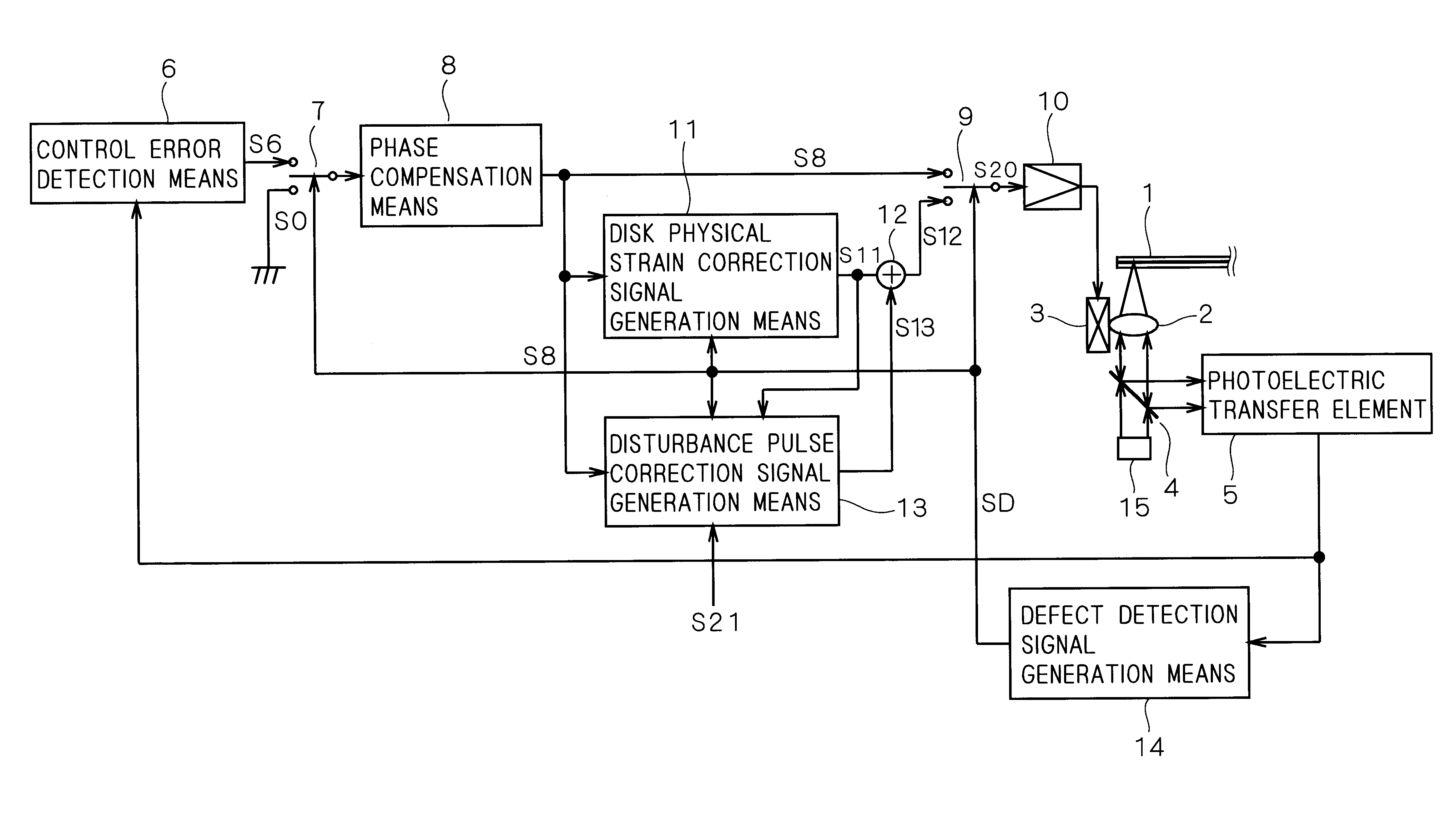
[0079]FIG. 4 is a block diagram that shows a construction of a disk device in accordance with the first preferred embodiment of the present invention. As illustrated in this Figure, a control loop switch 7, which receives an error signal S6 and a fixed electric potential signal S0 from an error detection means 6, supplies the fixed electric potential signal S0 to a phase compensation means 8 during the defect detection period indicating a defect detection state with the defect detection signal SD going “high”, while it supplies the error signal S6 to the phase compensation means 8 during the normal period indicating a normal state with the defect detection signal SD going “low”.

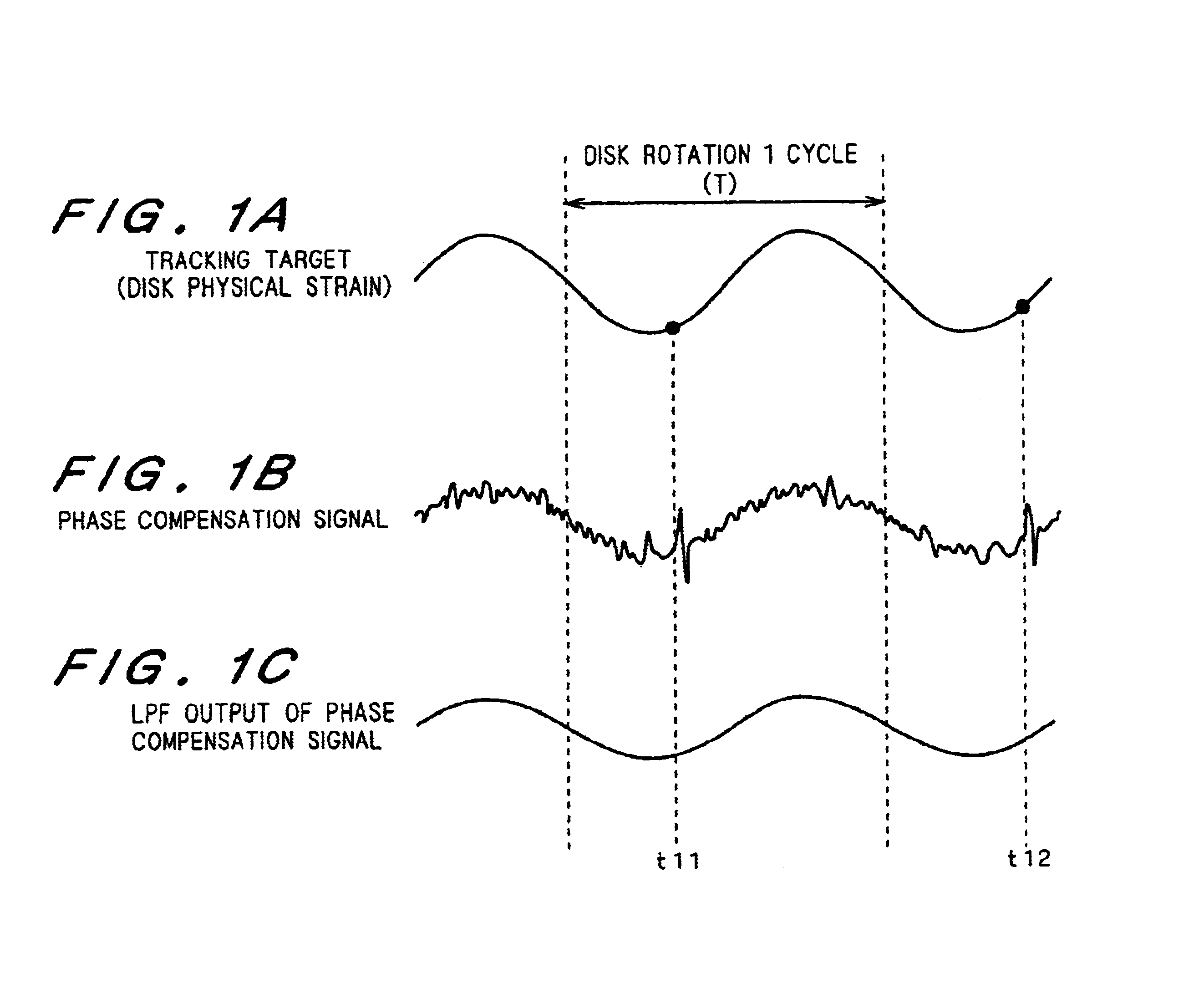
[0080]Based upon the signal obtained through a control loop switch 7, the phase compensation means 8 generates a phase compensation signal S8.

[0081]Upon receipt of the phase compensation signal S8 and the defect detection signal SD, the disk physical strain correction signal generation means 11 generates a di...

second preferred embodiment

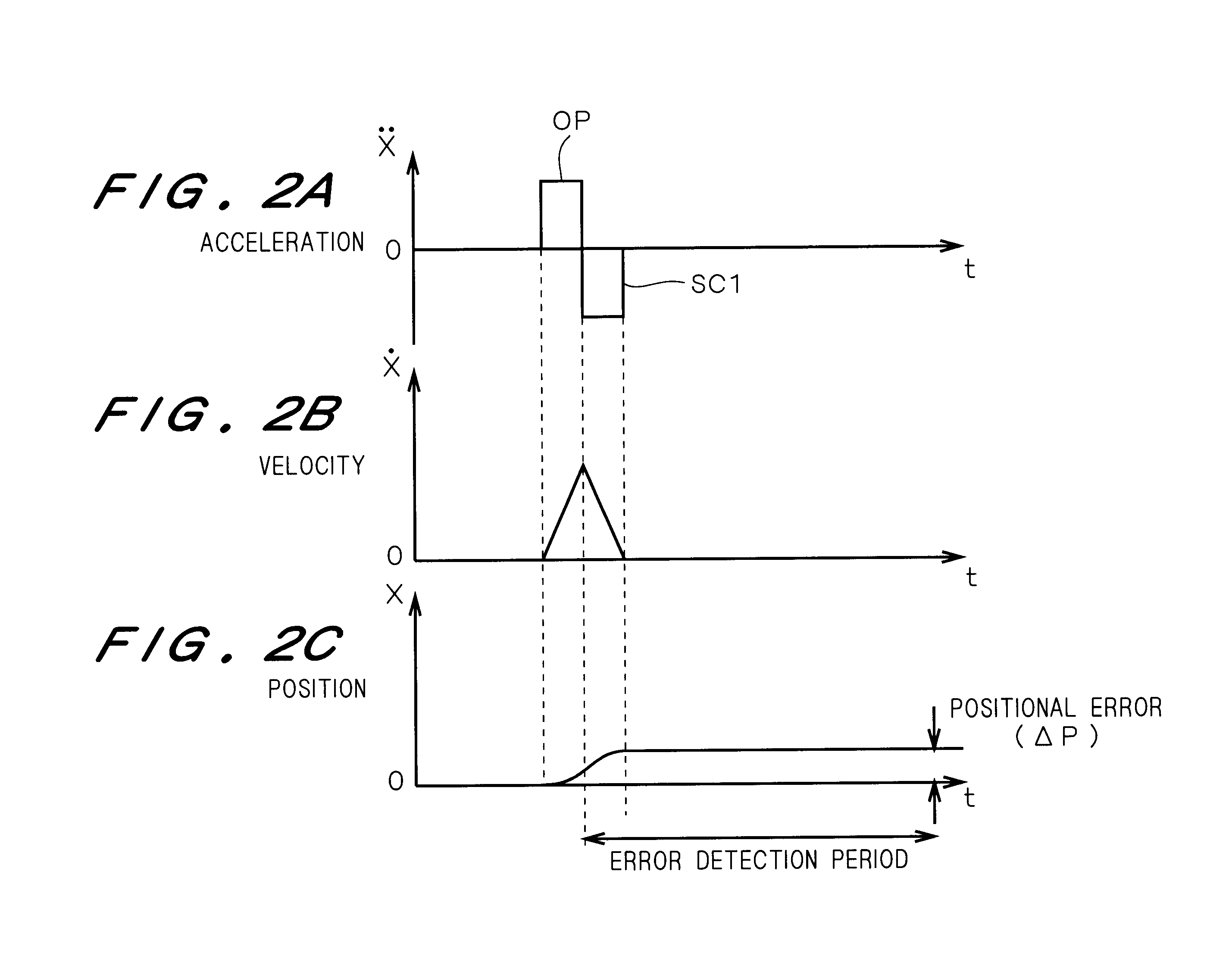
[0101]The second preferred embodiment relates to an optical disk device which can realize a defect compensation operation with higher precision. As already explained by reference to FIG. 3A to 3C, in the arrangement of the second preferred embodiment, the means (2) satisfying both the conditions (1) and (2) required for a stable, positive defect compensation is adopted, and with respect to the disturbance pulse correction signal, not only the correction pulse SC1, but also the correction pulses SC2 and SC3 are successively applied. The above-mentioned arrangement is realized by modifying the contents of the control of the memory output control means 13c in the first preferred embodiment in the following manner so as to satisfy the means (2).

[0102]In the same manner as the first preferred embodiment, the disturbance pulse memory means 13b of the second preferred embodiment is also constituted by n number of registers R0 to R(n−1), each having a predetermined bits. At the time when th...

third preferred embodiment

[0111]It has already been described that the disturbance pulse is caused by a disturbance error mixed into the error signal S6 at the defect start. Therefore, the time length of the disturbance pulse forms a function dependant on the reproducing linear velocity (linear velocity of the disk 1 at the time of reproduction), and it is clear that as the linear velocity becomes faster, the time length of the disturbance pulse becomes shorter and as the linear velocity becomes slower, the time length of the disturbance pulse becomes longer. Consequently, it is preferable to vary the disturbance pulse memory time in response to the linear velocity. In other words, the third preferred embodiment realizes an optical disk device that can store disturbance pulses accurately.

[0112]The optical disk device of the third preferred embodiment has the same structure as that of the first and second preferred embodiments, except that only the construction of the disturbance pulse correction signal gener...


PUM

PropertyMeasurementUnit
defectaaaaaaaaaa
frequencyaaaaaaaaaa
linear velocityaaaaaaaaaa

Abstract

A disk physical strain correction signal generator outputs a signal obtained by allowing a phase compensation signal to pass a LPF as a disk physical strain correction signal during a normal period. During a defect detection period, it outputs the output signal of the LPF sampled at the time of the defect detection start as the disk physical strain correction signal. A disturbance pulse correction signal is output based upon a disturbance pulse obtained by subtracting the disk physical strain correction signal from the phase compensation signal. The disk physical strain correction signal and the disturbance pulse correction signal are added to output a defect compensation signal. This defect compensation signal is applied as an actuator control signal during the defect detection period. Thus, it is possible to provide an optical disk device which can carry out a stable driving control for a reproducing operation, etc. without losing the continuity of control before and after the defect detection even when the defect detection period is long.

Description

BACKGROUND OF THE INVENTION[0001]1. Field of the Invention[0002]The present invention relates to an optical disk device such as a DVD and a CD, and more particularly concerns a control system which can cancel adverse effects caused by a defect located on the optical disk.[0003]2. Description of the Background Art[0004]In optical disk apparatuses, various methods for reproducing data from a disk in spite of defects such as scratches and stain (hereinafter, referred to as “defective disks”) located thereon have been proposed, and for example, Japanese Patent Application Laid-Open No. 11-259871(1999) discloses a method in which upon reproducing data from a defective disk, the data is reproduced while interpolating error signals.[0005]FIG. 13 is a block diagram that schematically shows a construction (first construction) of a conventional defect compensating device for defective disks in accordance with the above-mentioned publication.[0006]As illustrated in the Figure, a laser light be...

Claims


Application Information

Patent Timeline
Patent Type & Authority Patents(United States)
IPC IPC(8): G11B7/09G11B7/095G11B20/18G11B19/02
CPCG11B7/0948G11B7/0953G11B7/0956G11B20/18G11B19/02
Inventor YOKOYAMA, EIJIRYU, TOMOAKI
Owner MITSUBISHI ELECTRIC CORP
Why Eureka
Try Eureka