
Waveguide stress engineering and compatible passivation in planar lightwave circuits

Inactive Publication Date: 2005-09-20
LUMENTUM OPERATIONS LLC
View PDF11 Cites 3 Cited by
  • Summary
  • Abstract
  • Description
  • Claims
  • Application Information

AI Technical Summary

Benefits of technology

[0011]The passivation layer has the requisite passivation properties (i.e., protection against environmental conditions against which the devices will be tested), and is compatible with the stress management used in lower circuit layers.

Problems solved by technology

AWGs however are thin, fragile chips with narrow waveguides produced using planar lightwave circuit (PLC) processing techniques.
The various processing tolerances required to meet the requisite optical specifications are already very tight, and in fact get tighter as the need to process more and closer channels increases.
Stress-induced birefringence in waveguides leads to unacceptably high polarization dependent loss (PDL) for communication systems.
Because the materials used for these layers are different, with differing properties (e.g., differing coefficients of thermal expansion (CTEs)), intra-and inter-layer stresses exist and will result in high levels of waveguide PDL.
Even assuming that such techniques are employed to manage stress, they are still susceptible to the adverse environmental conditions, discussed above.
Modified annealing techniques for the overcladding have been proposed, but have not produced satisfactory protection.
Hermetic packaging of the circuits can also provide protection, but such techniques can be expensive, and subject to long-term failures.

Method used


Image

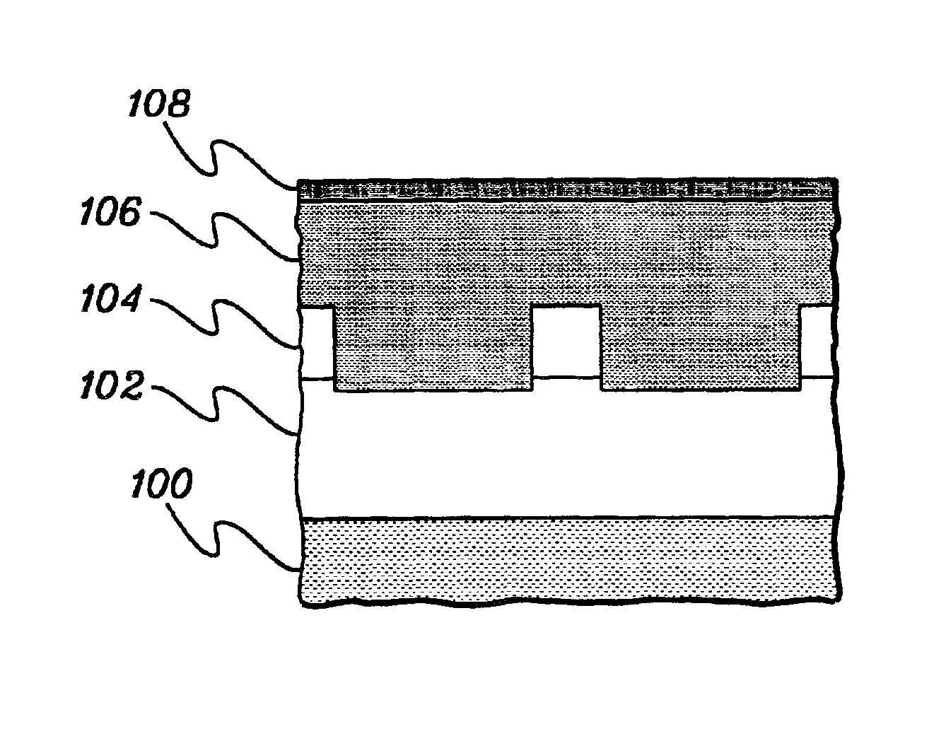
  • Waveguide stress engineering and compatible passivation in planar lightwave circuits
  • Waveguide stress engineering and compatible passivation in planar lightwave circuits
  • Waveguide stress engineering and compatible passivation in planar lightwave circuits

Examples


Embodiment Construction

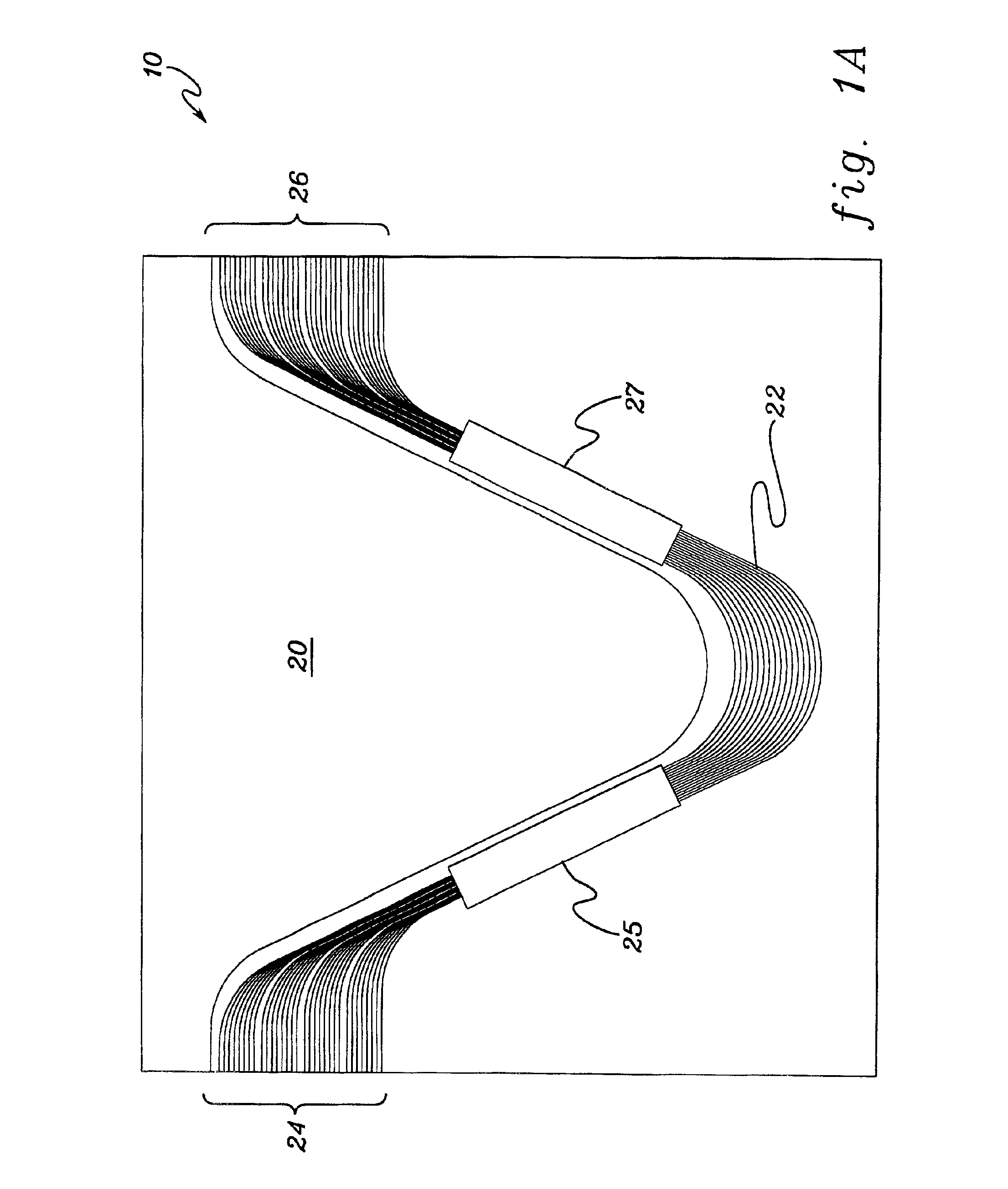
[0024]With reference to FIG. 1A, an exemplary planar lightwave circuit (PLC) 10 is shown in the form of an arrayed waveguide grating (AWG) formed over a substrate 20 (e.g., silicon). As known to those in the art, an AWG uses an array of closely spaced waveguides 22 having carefully controlled, differing path lengths which cause constructive phase interference patterns on the respective optical signals transmitted into and out of the device. This technique is useful for multiplexing or demultiplexing optical signals passed between the array input / focusing region 24 / 25 to the array output / focusing region 26 / 27. The tight spatial and thermal tolerances necessary for proper operation of array 20, as discussed above, lead to the requirements for effective packaging and sealing for use in adverse environmental conditions. Moreover, as discussed above, waveguides 22 are highly susceptible to stresses, thus imposing the additional requirement of stress engineering during their fabrication.

[...


PUM


Abstract

A planar lightwave circuit includes at least one optical waveguide core, and at least one feature proximate the core having a stress-engineered property to balance stress and therefore minimize birefringence affecting the core. A protective passivation layer is formed over the core and the feature to be substantially non-interfering with the balanced stress provided by the feature. The stress balancing feature may be an overcladding layer formed over the core, doped to have a coefficient of thermal expansion approximately matched to that of an underlying substrate, to symmetrically distribute stress in an undercladding between the overcladding and the substrate, away from the core. The protective passivation layer is formed to have a coefficient of thermal expansion approximately matched to that of the overcladding. In one exemplary embodiment, the passivation layer is formed from silicon nitride. Related concepts of stress release grooves, and core overetching, are also disclosed.

Description

FIELD OF THE INVENTION[0001]The present invention relates to protective passivation layers for planar lightwave circuits. More particularly, the present invention relates to passivation techniques which preserve the stress engineered environment of underlying optical waveguide layers.BACKGROUND OF THE INVENTION[0002]Fiber optic communication links have been conventionally employed in long-haul, point-to-point networks with controlled environments at all interface points. Such highly controlled, “central office” surroundings usually offer relatively benign operating environments (temperature, humidity, mechanical) for components. Consequently, highly functional components could be developed and installed without considering the impact of other, more extreme environments.[0003]Recent technological advances, coupled with increasing bandwidth demand, are rapidly expanding the use of fiber optic components beyond the “central office” and into potentially harsher environments. For example...

Claims


Application Information

Patent Timeline
IPC IPC(8): G02B6/13G02B6/136G02B6/12G02B6/34
CPCG02B6/1203G02B6/13G02B6/136G02B2006/12097G02B2006/12176
Inventor BHARDWAJ, JYOTI KIRONBRAINARD, ROBERT JAMESDONG, ZI-WENDOUGHERTY, DAVIDEGAN, ERIK W.GOPINATHAN, NIRANJANNAKAMOTO, DAVID K.NGUYEN, THOMAS THUANTHEKDI, SANJAY M.VAIDYANATHAN, ANANTHARAMANYAMADA, HIROAKIYAN, YINGCHAO
Owner LUMENTUM OPERATIONS LLC
Learn More