Method of dividing wafer

Active Publication Date: 2006-07-27
DISCO CORP
View PDF3 Cites 11 Cited by
  • Summary
  • Abstract
  • Description
  • Claims
  • Application Information

AI Technical Summary

Benefits of technology

[0011] When a grinding step of grinding the back of the wafer is performed before the resist film coating step, it is preferable that etching is further performed after the resist film has been removed in the division step in order to remove stress in the backs of the individual devices produced in the grinding step. For example, the resist film contains any one of polyimide resin, epoxy resin, and acrylic resin.
[0012] In the invention, using a property of the resist film that can be etched in spite of a low etching rate, a resist agent is removed in a degree of eliminating need of ashing at the same time when dicing by etching has been completed. Therefore, a step of removing the resist film is unnece

Problems solved by technology

However, there has been a problem that since such cutting is performed by crushing the streets using a cutting blade rotated at high speed, the blade containing grinding particles such as diamond particles hardened by nickel plating and the like and being formed to be approximately 20 μm in thickness, therefore small chips appear on a cuttin

Method used


Image

  • Method of dividing wafer
  • Method of dividing wafer
  • Method of dividing wafer

Examples


Example

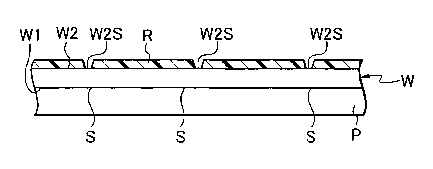
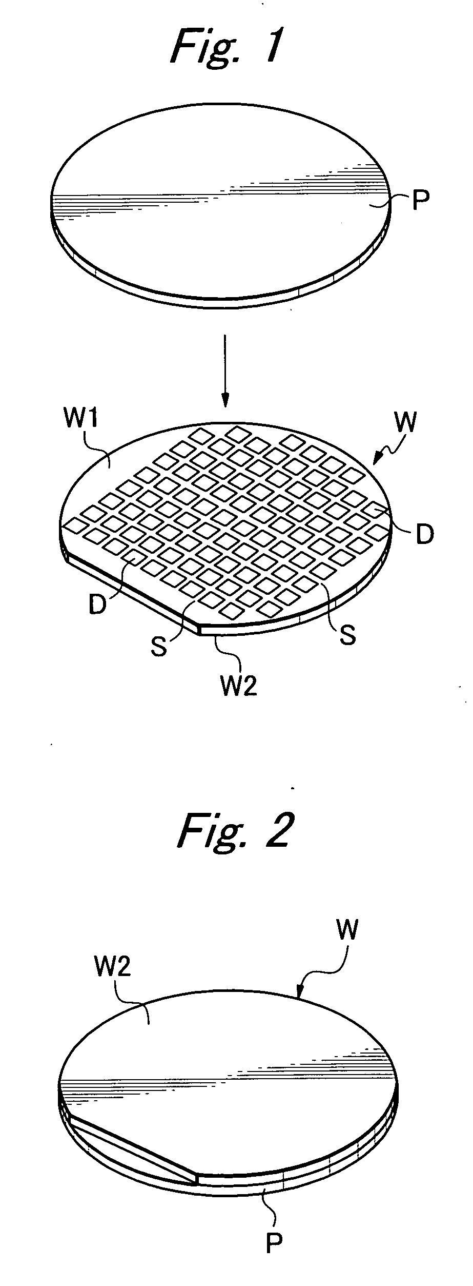
[0025] A plurality of devices D is formed with being partitioned by streets S on a surface W1 of a wafer W as shown in FIG. 1. First, as shown in FIG. 1, a protection member P for protecting the devices D is adhered to the surface W1 of the wafer W. As the protection member P, a hard plate such as a glass plate, polyethylene terephthalate plate, or ceramic plate is used, in addition, an adhesion tape can be used.

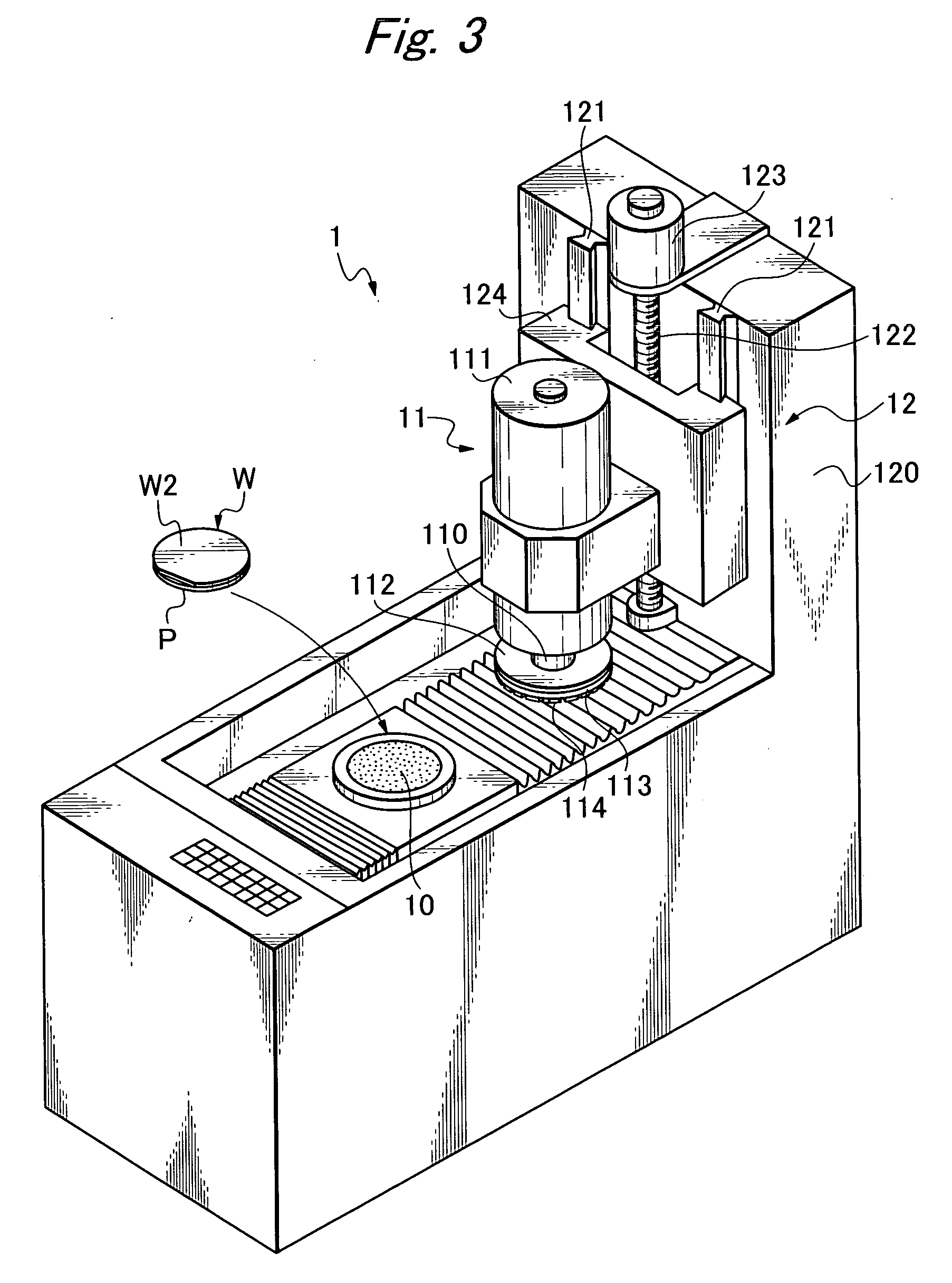
[0026] Next, as shown in FIG. 2, a back W2 of the wafer W having the surface W1 to which the protection member P has been adhered is directed upward, and then the back W2 is ground to have a certain thickness. In such grinding, for example, a grinding machine 1 as shown in FIG. 3 can be used. The grinding machine 1 has a chuck table 10 for holding the wafer, a grinding unit 11 for grinding the wafer held by the chuck table 10, and a grinding feed unit 12 for moving the grinding unit 11 closer or farer with respect to the chuck table 10.

[0027] The grinding unit 11 is config...


PUM


Abstract

To eliminate necessity of separation of a resist film in dicing by etching and thus improve productivity and die strength of a device, thickness of the resist film is adjusted such that when street-correspondent-areas are separated by etching, resist films coated on portions other than the street-correspondent-areas are not remained.

Description

BACKGROUND OF THE INVENTION [0001] 1. Field of the Invention [0002] The present invention relates to a method of dividing a wafer. [0003] 2. Related Art [0004] A wafer having a plurality of devices formed at a surface side with being partitioned by streets is formed to be in a certain thickness by back grinding, and then subjected to dicing by cutting along the streets, thereby divided into individual devices for use in various electronic instruments. [0005] However, there has been a problem that since such cutting is performed by crushing the streets using a cutting blade rotated at high speed, the blade containing grinding particles such as diamond particles hardened by nickel plating and the like and being formed to be approximately 20 μm in thickness, therefore small chips appear on a cutting surface (side face) of the device, which reduces die strength of the device. In particular, when thickness of the wafer is decreased to 100 μm or less, or further decreased to 50 μm or less...

Claims


Application Information

Patent Timeline
IPC IPC(8): H01L21/78
CPCH01L21/78
Inventor ONO, TAKASHI
Owner DISCO CORP
Why Eureka
Try Eureka