Microbolometer focal plane array with temperature compensated bias

a microbolometer and focal plane array technology, applied in the field of imaging systems employing microbolometer focal plane arrays, can solve the problems of difficult processing of roic output signals, inability to meet the needs of microbolometer array roics, and individual microbolometer pixels will have non-uniform responses to uniform incident infrared radiation

Inactive Publication Date: 2005-10-11
JOHN FLUKE MFG CO INC
View PDF1 Cites 21 Cited by
  • Summary
  • Abstract
  • Description
  • Claims
  • Application Information

AI Technical Summary

Benefits of technology

[0019]An object of the present invention is to provide a simple method for correcting for temperature induced errors in microbolometer focal-plane arrays.

Problems solved by technology

Individual microbolometer pixels will have non-uniform responses to uniform incident infrared radiation, even when they are manufactured as part of a single microbolometer FPA.
The resulting ROIC output signal is difficult to process, as it requires system interface electronics having a very high dynamic range.
The current state-of-the-art in microbolometer array ROICs suffers from two principal problems.
The first problem is that the larger arrays increase substrate temperature.
A second problem is that a larger microbolometer introduces non-uniformities in the ROIC integrated circuit output signal thereby requiring a large instantaneous dynamic range in the sensor interface electronics that increases the cost and complexity of the system.
Although the aforesaid patent sets forth improved methods for correcting temperature induced errors in microbolometer focal-plane arrays, these methods still remain complex and time consuming.
Another source of error in microbolometer focal plane arrays is the variation in “responsivity” of each microbolometer with changes in temperature.

Method used


Image

  • Microbolometer focal plane array with temperature compensated bias
  • Microbolometer focal plane array with temperature compensated bias
  • Microbolometer focal plane array with temperature compensated bias

Examples


Embodiment Construction

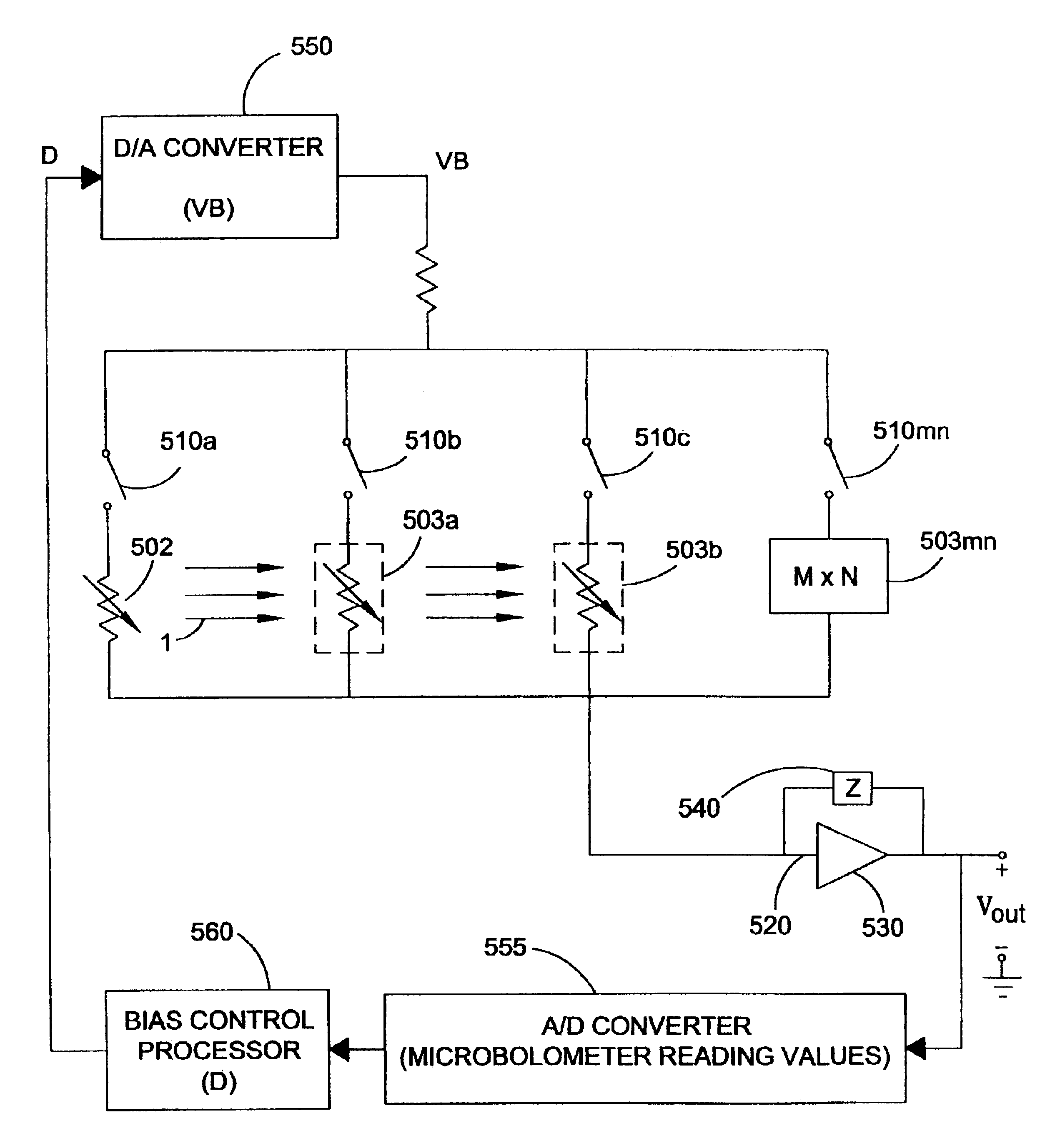
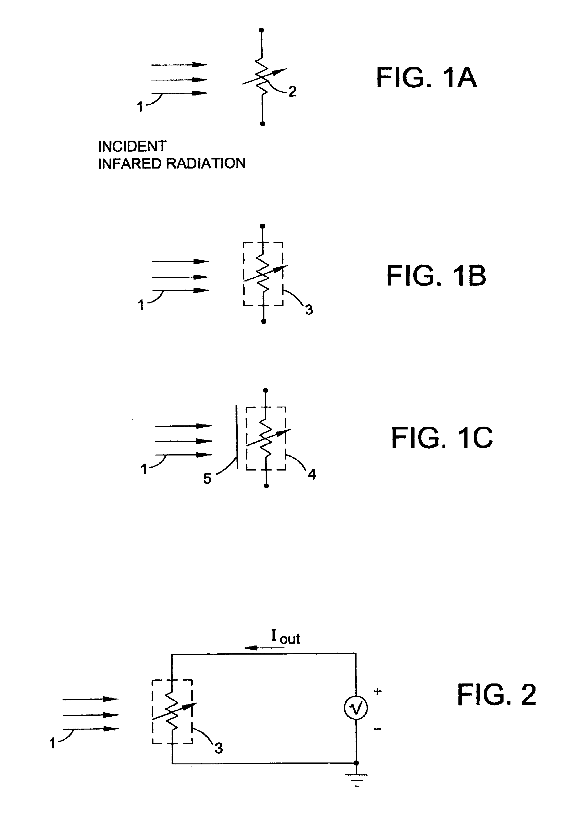
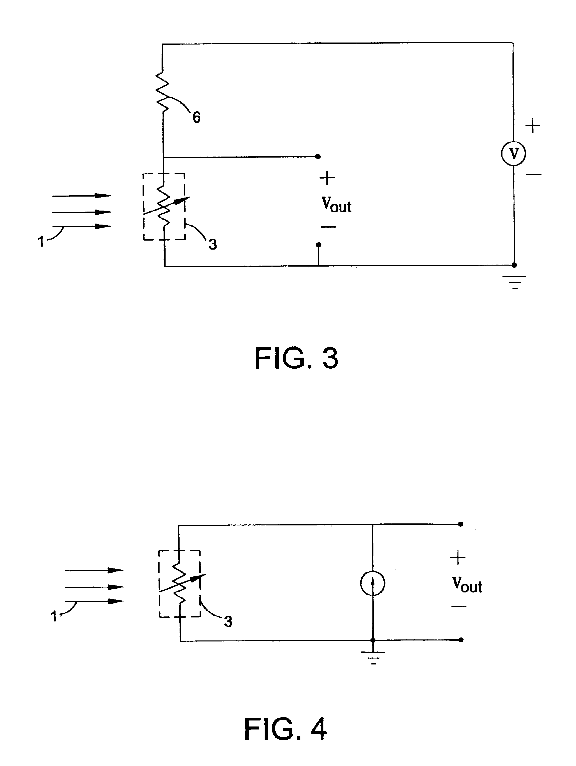
[0043]Constructions of microbolometer focal plane arrays and application circuitry are taught in the aforesaid U.S. Pat. No. 5,756,999 and is incorporated herein by reference. Individual microbolometer detectors including both thermally-isolated and thermally-shorted varieties, and associated detector circuitry are also described in detail therein. However, the following excerpt is provided as a foundation for the description of the present invention that follows:

[0044]“FIGS. 1A, 1B and 1C illustrate three possible configurations for microbolometer detectors. Incident infrared radiation 1 is projected onto each of the microbolometer detectors. The microbolometer detector 2, shown in FIG. 1A, is thermally shorted to the substrate material, herein referred to as the thermally-shorted microbolometer or heat sunk pixel. This is a common form of bolometer and is representative of most single-detector bolometers and thermistors. Microbolometers can be manufactured to provide a high therma...


PUM


Abstract

A readout circuit for an array of substrate-isolated microbolometer detectors includes a bias source that varies in accordance with changes in substrate temperature as detected by a temperature sensor that has temperature characteristic that resembles the temperature characteristic of the microbolometer detector array so as compensate detector measurements for temperature induced errors in the microbolometer focal plane array read out.

Description

RELATED APPLICATIONS[0001]This application is a continuation in part of U.S. application Ser. No. 10 / 198,295, filed 5 Jul. 2002 now U.S. Pat. No. 6,538,250, which is a continuation of U.S. application Ser. No. 09 / 414,688, filed 7 Oct. 1999, now U.S. Pat. No. 6,444,983, the disclosures of which are hereby incorporated in their entirety by reference herein.FIELD OF THE INVENTION[0002]The present invention relates generally to imaging systems employing a microbolometer focal plane array. More specifically, the present invention is directed to methods and circuitry for correcting temperature-induced errors in a microbolometer focal plane arrays.BACKGROUND OF THE INVENTION[0003]An infrared detector called the “bolometer,” now well known in the art, operates on the principle that the electrical resistance of the bolometer material changes with respect to the bolometer temperature, which in turn changes in response to the quantity of absorbed incident infrared radiation. These characterist...

Claims


Application Information

Patent Timeline
Patent Type & Authority Patents(United States)
IPC IPC(8): G01J5/00G01J5/24
CPCG01J5/22G01J5/24H04N5/33H04N25/673H04N25/671
Inventor ANDERSON, SHANE M.MCMANUS, TIMOTHY J.
Owner JOHN FLUKE MFG CO INC
Why Eureka
Try Eureka