

Substrate process tank with acoustical source transmission and method of processing substrates
a technology of substrate and transmission channel, applied in the direction of cleaning using liquids, transportation and packaging, packaging, etc., can solve the problems of reducing production time, reducing the production capacity of substrate devices, and increasing the miniaturization of semiconductor devices
- Summary
- Abstract
- Description
- Claims
- Application Information
AI Technical Summary
Benefits of technology
Problems solved by technology
Method used
Image

Examples
first embodiment
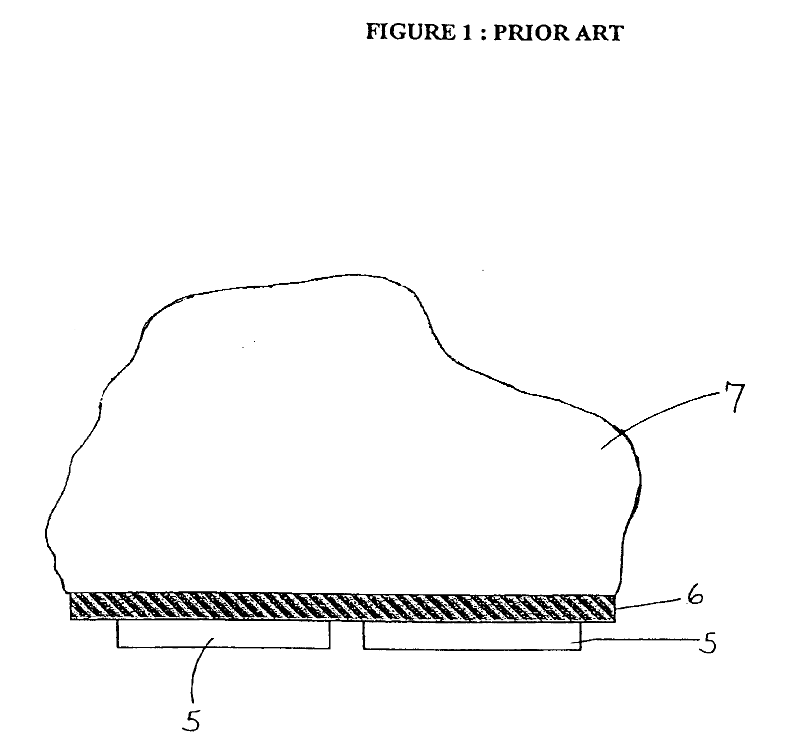
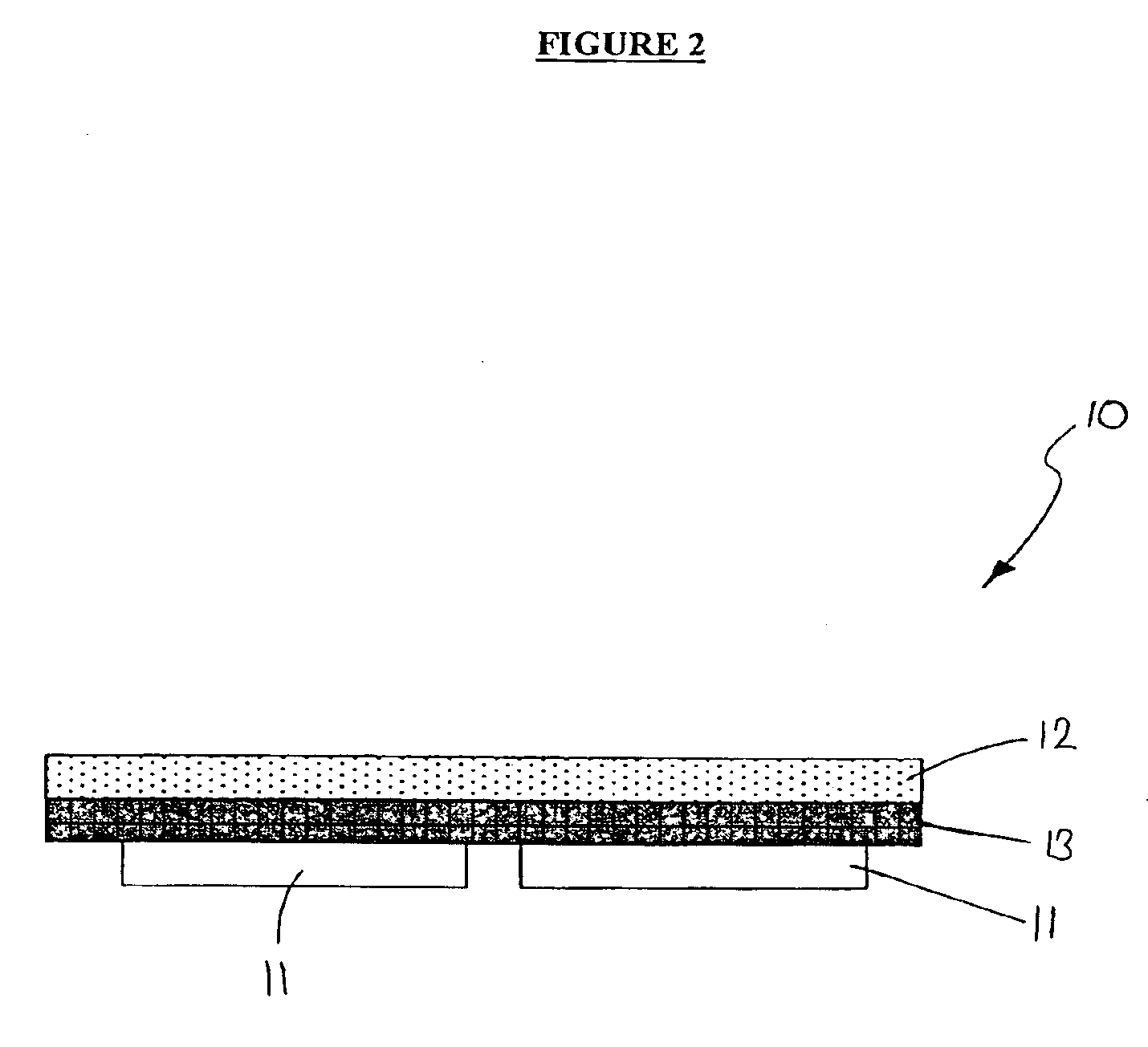
[0029]Referring to FIGS. 2 and 3, acoustical stack 10 is schematically illustrated according to the present invention. Acoustical stack 10 comprises two piezoelectric crystals 11, rigid plate 12, and transmission layer 13. Transmission layer 13 is positioned between piezoelectric crystals 11 and rigid plate 12. Piezoelectric crystals 11 are bonded to one side of transmission layer 13 while rigid plate 12 is bonded to the other side of transmission layer 13. Bonding is accomplished through the use of a bonding agent, such as epoxy. Once the acoustical stack 10 is assembled, acoustical stack 10 is coupled to a process chamber 20 so that the side of rigid plate 12 that is not bonded to the transmission layer 13 is in direct contact with that process fluid 21 that fills the process chamber 20. When crystals 11 are activated to produce acoustical energy, acoustical stack 10 will act as an acoustical energy pathway form the crystals 11 to the process fluid 21. When a substrate 22 is subme...
second embodiment
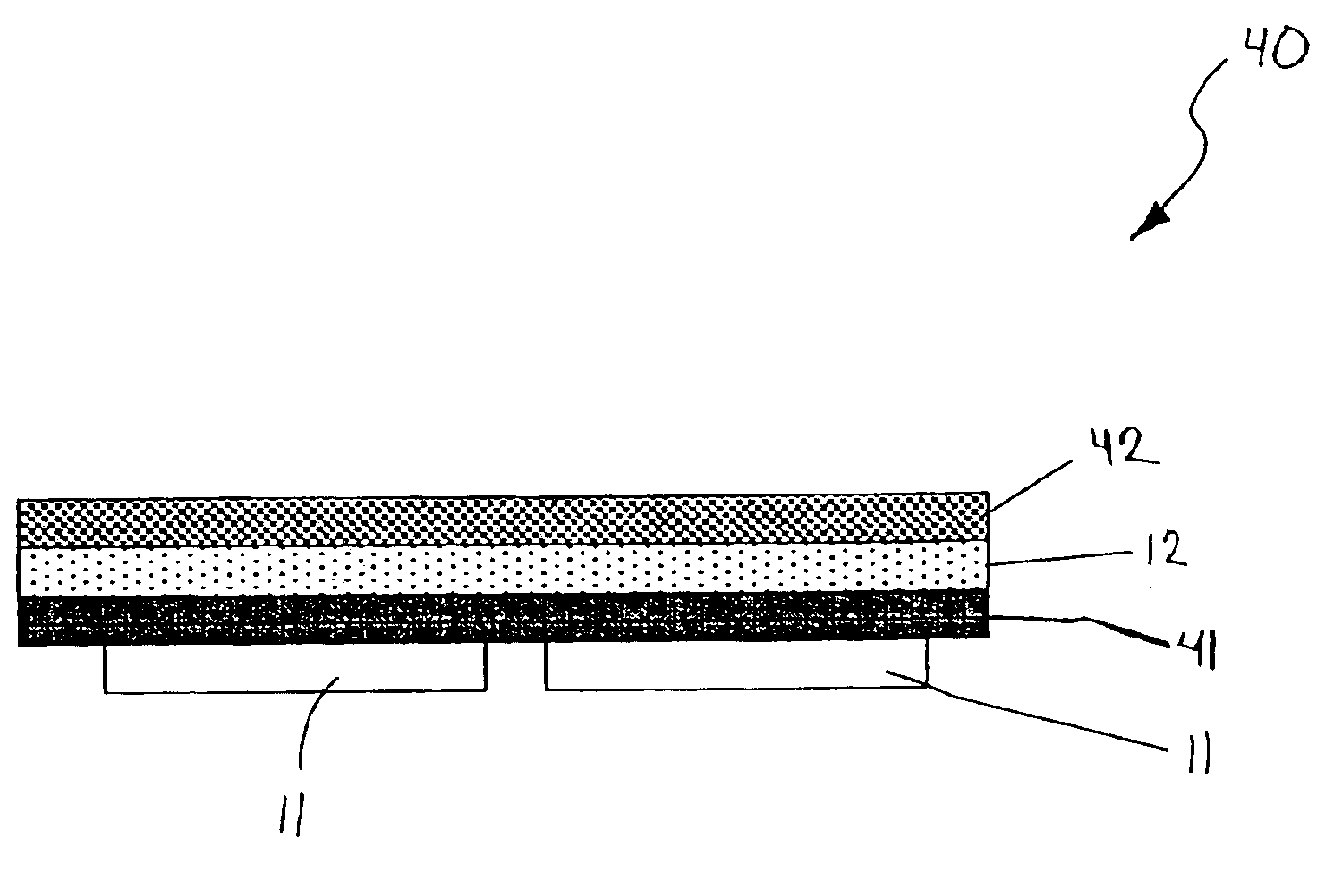
[0033]Turning now to FIG. 4, acoustical stack 40 is illustrated according to the present invention. Acoustical stack 40 comprises first transmission layer (“TL 1”) 41 positioned between the crystals 11 and the rigid plate 12. Acoustical stack 40 also has a second transmission layer (“TL 2”) 42 positioned on the other side of the rigid plate 12. When acoustical stack 40 is coupled to a process chamber, similar to the coupling illustrated in FIG. 3 for acoustical stack 10, the second transmission layer 42 of acoustical stack 40 will be in contact with the process fluid. In this embodiment, the first and second transmission layers 41, 42 are used to more gradually transition the Za between the crystals 11 and the process fluid. The system is designed so that ZaCystal>ZaTL1>ZaRigid Plate>ZaTL2>ZaProcess Fluid. In this embodiment, preferably, crystals 11 are piezoelectric crystals, first transmission layer 41 is made of aluminum, titanium, or beryllium, rigid plate 12 is a quartz plate, ...
third embodiment
[0034]Referring now to FIG. 5, acoustical stack 50 is illustrated according to the present invention. Acoustical stack 50 comprises a single transmission layer 51 coupled to one side of rigid plate 12. When coupled to a process chamber, transmission layer 51 will be between the rigid plate 12 and the process fluid. In this embodiment, a single transmission layer 51 is used to more gradually transition the Za between the rigid plate 12 and the process fluid. The acoustical stack 50 is designed so that ZaCrystalRigid Plate>ZaTransmission Layer>ZaProcess Fluid. In this embodiment, crystals 11 can be piezoelectric crystals, rigid plate 12 can be made of stainless steel, and transmission layer 51 can be made of PCTFE, ECTFE, FEP, PFA, teflon, or other fluorocarbon-based polymers or thermoplastic polymers. This embodiment does not follow the Za step down rule one hundred percent, but the transmission layer still provides improved transmission from the stainless steel plate to the process ...
PUM
| Property | Measurement | Unit |
|---|---|---|
| acoustical energy | aaaaa | aaaaa |
| acoustical impedance | aaaaa | aaaaa |
| transmission | aaaaa | aaaaa |
Abstract
Description
Claims
Application Information