Test method and apparatus for verifying fabrication of transistors in an integrated circuit

a technology of integrated circuit and test method, which is applied in the direction of pulse generator, pulse technique, instruments, etc., can solve the problems of large scale ic to operate out of designed specification, apparatus may not detect the presence of any failure of n-channel and/or p-channel mosfets, and the performance of the integrated circuit device is degraded

Active Publication Date: 2005-10-25
RENESAS ELECTRONICS CORP
View PDF11 Cites 53 Cited by
  • Summary
  • Abstract
  • Description
  • Claims
  • Application Information

AI Technical Summary

Problems solved by technology

Poor formation of such transistors during fabrication leads to degraded performance of the integrated circuit device.
There is a problem that this conventional test method and apparatus may not detect the presence of any failure of n-channel and / or p-channel MOSFETs to meet the preselected deviation specifications of large scale IC (LSI) being verified.
Under this operating condition, if, in a circuit portion relying heavily on operating speed of n-channel and / or p-channel MOSFETs, rising time or falling time of them is longer in excess of a preselected deviation specification, this circuit portion may cause a large scale IC to operate out of designed specification.
The conventional test method and apparatus cannot detect the above-mentioned failure in original circuit components.

Method used


Image

  • Test method and apparatus for verifying fabrication of transistors in an integrated circuit
  • Test method and apparatus for verifying fabrication of transistors in an integrated circuit
  • Test method and apparatus for verifying fabrication of transistors in an integrated circuit

Examples


Embodiment Construction

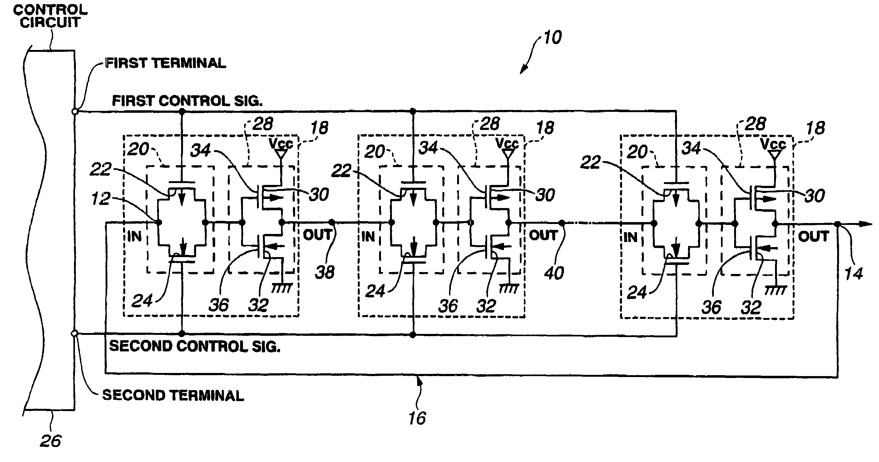
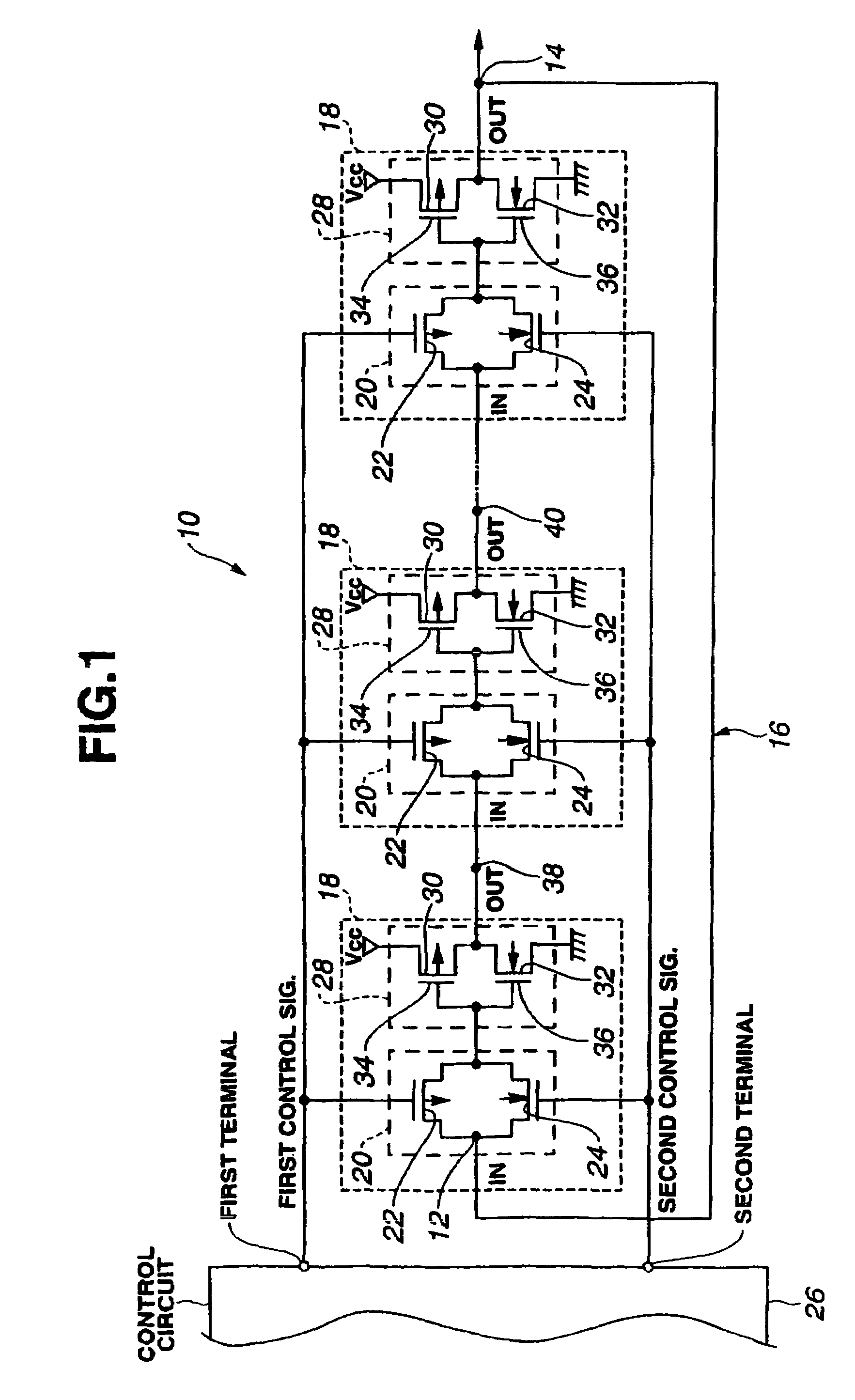
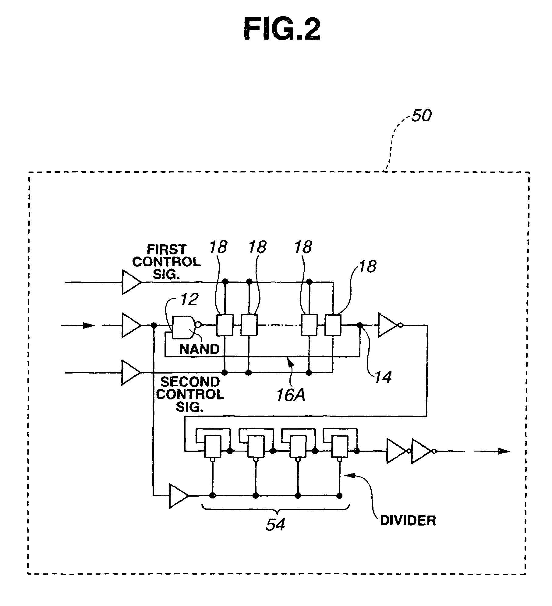
[0043]The present invention is directed to a test method and an associated apparatus for verifying fabrication of transistors of the first and second conductivity types (e.g., n-channel MOSFETs and p-channel MOSFETs) constituting basic components of an integrated circuit IC on a die under test. The test apparatus includes a voltage controlled ring oscillator provided on the die being verified during fabrication of the IC. The ring oscillator has a structure including n-channel MOSFETs and p-channel MOSFETs of the IC. The n-channel and p-channel MOSFETs and their interconnection to make the ring oscillator are formed, for example, during the fabrication of diffusion, metal and polysilicon regions and vias / contacts between these regions that are used to fabricate the IC on a wafer. In exemplary implementations of the present invention discussed below, the ring oscillator is coupled to an external control circuit. The control circuit shifts a two-level first control voltage signal and ...


PUM


Abstract

A ring oscillator for a test apparatus and method for verifying fabrication of transistors in an integrated circuit on a die under test is implemented. The ring oscillator is fabricated on the die and includes a positive feedback loop between a circuit output terminal and a feedback input terminal. The feedback loop includes a plurality of delaying stages connected in cascade. A transfer gate is coupled to each delaying stage. Each of the transfer gates includes a pair of transistors of the first and second conductivity types connected in parallel. The ring oscillator is operable to provide a first oscillator output signal during a first test mode when the transistors of the first conductivity type are ON and the transistors of the second conductivity type are OFF. The ring oscillator is operable to provide a second oscillator output signal during a second test mode when the transistors of the first conductivity type are OFF and the transistors of the second conductivity type are ON. The ring oscillator is operable to provide a third oscillator output signal during a third test mode when the transistors of the first conductivity type are ON and the transistors of the second conductivity type are ON.

Description

FIELD OF THE INVENTION[0001]The present invention relates to the fabrication of integrated circuit devices, and in particular to test methods and apparatuses for verifying fabrication of transistors in an integrated circuit device.DESCRIPTION OF THE RELATED ART[0002]P-channel and n-channel metal oxide semiconductor field effect transistors (MOSFETs) are used in modern integrated circuit (IC) devices. Poor formation of such transistors during fabrication leads to degraded performance of the integrated circuit device. Consequently, there is a need in the art for test methods and apparatuses to verify that satisfactory performance of the circuit has been achieved.[0003]Existing test method and apparatus measures a period of a ring oscillator provided on a die being verified and compares the period to a predetermined specification. The ring oscillator for the die under test and circuitry thereon are formed during the same process steps. One example of test apparatus is described in Publ...

Claims


Application Information

Patent Timeline
Patent Type & Authority Patents(United States)
IPC IPC(8): G01R31/27G01R31/26H03K3/03H03K3/00H03K3/354
CPCG01R31/275G01R31/2884H03K3/0315
Inventor NAKAJIMA, KAZUHIRO
Owner RENESAS ELECTRONICS CORP
Why Eureka
Try Eureka