Storage structure with cleaved layer

a storage structure and cleaved layer technology, applied in the direction of basic electric elements, electrical apparatus, semiconductor devices, etc., can solve the problems of reducing the size of the photolithography, affecting the yield of the product, and the photolithography is nearing the x-ray energy level,

Inactive Publication Date: 2005-11-22
HEWLETT PACKARD DEV CO LP
View PDF22 Cites 207 Cited by
  • Summary
  • Abstract
  • Description
  • Claims
  • Application Information

AI Technical Summary

Problems solved by technology

Photolithography is nearing X-ray energy levels, however, and is encountering limits in further size reductions.
Three-dimensional semiconductor-based structures have provided additional opportunities to increase density, but error probabilities are multiplied as the number of stacked layers increases, and statistics of yield quickly become unsatisfactory.
Crystals cannot easily be stacked on top of amorphous or non-crystalline oxides, because crystal growth on top of a disordered substrate impedes proper registration of new atoms across the surface and often results in polycrystalline material.
Additionally, once a device and a layer have been created, it is generally deleterious to subject them to further thermal input, as is often needed when a next layer is being formed.
These and other challenges increase the difficulties and costs associated with stacked devices.

Method used


Image

  • Storage structure with cleaved layer
  • Storage structure with cleaved layer
  • Storage structure with cleaved layer

Examples


Embodiment Construction

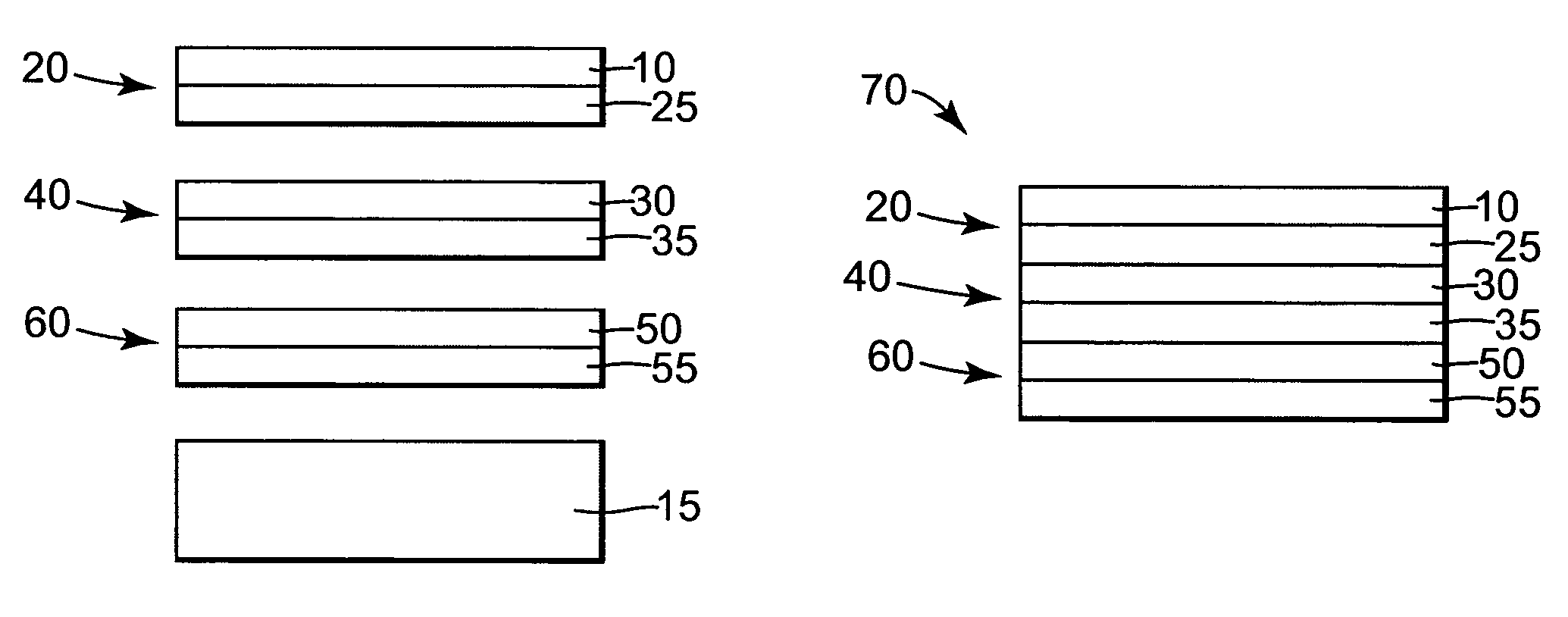
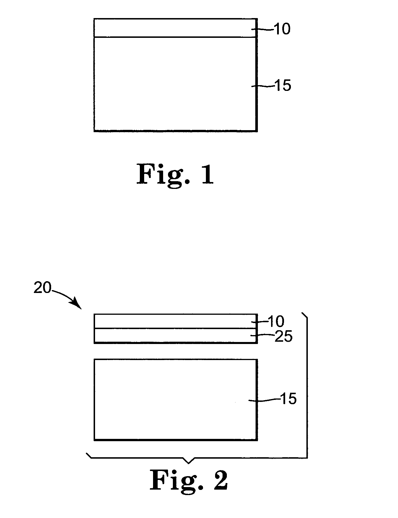
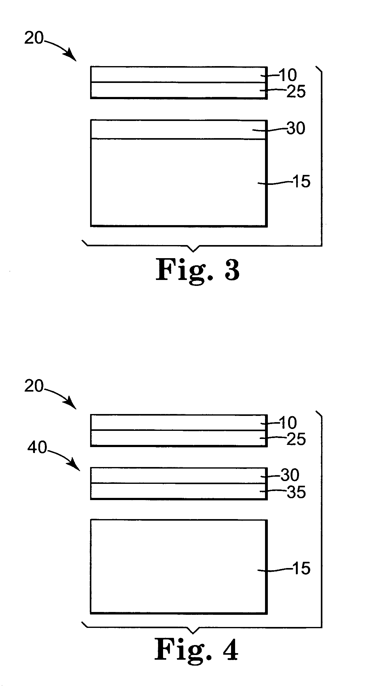
[0016]A method of making a multi-layered memory or other electronic storage structure according to an embodiment of the invention includes forming device layer 10 on single-crystal silicon wafer 15, as shown in FIG. 1. Device layer 10 includes devices such as diodes, transistors, antifuses, tunnel junctions, etc., which are implanted, deposited, or otherwise formed or provided in layer 10. Other examples of such devices include, but are not limited to, charge-coupled devices (CCDs), complementary metal oxide semiconductor (CMOS) imagers and other CMOS devices, tunnel diodes, charge pumps, and other devices.

[0017]As shown in FIG. 2, the method further includes cleaving device layer 10 from wafer 15. Cleaved portion 20 includes device layer 10 and cleaved wafer section 25. Ion-implantation induced layer splitting of wafer 15, for example, using hydrogen or other light species, accomplishes the cleaving of portion 20 from wafer 15. The hydrogen or other ion penetrates to a desired dept...


PUM


Abstract

Apparatus and method for making a multi-layered storage structure includes forming a device layer on a single-crystal wafer, cleaving the device layer from the wafer, repeating the forming and cleaving to provide a plurality of cleaved device layers, and bonding the cleaved device layers together to form the multi-layered storage structure.

Description

BACKGROUND OF THE INVENTION[0001]The demand for semiconductor devices has increased dramatically over the years. Many frequently used electronic devices are made possible because of developments in semiconductor devices. As such devices become smaller, more sophisticated, and less expensive, the marketplace demands increasingly higher circuit densities, increased performance, and lower cost.[0002]Increasing the density of semiconductor devices has been accomplished by reducing associated component area. Photolithography is nearing X-ray energy levels, however, and is encountering limits in further size reductions. Three-dimensional semiconductor-based structures have provided additional opportunities to increase density, but error probabilities are multiplied as the number of stacked layers increases, and statistics of yield quickly become unsatisfactory.[0003]Crystal-based semiconductor devices generally provide better results than other devices, because regular arrays of atoms pro...

Claims


Application Information

Patent Timeline
Patent Type & Authority Patents(United States)
IPC IPC(8): H01L21/762H01L21/20H01L21/70H01L21/02H01L27/10H01L21/8246H01L27/105H01L27/12
CPCH01L21/2007H01L21/76254
Inventor MEYER, NEAL W.VAN BROCKLIN, ANDREW L.FRICKE, PETERJACKSON, WARRENELDREDGE, KENNETH JAMES
Owner HEWLETT PACKARD DEV CO LP
Why Eureka
Try Eureka