VLSI-photonic heterogeneous integration by wafer bonding

a technology of wafer bonding and photonics, applied in the field of optical and electronic chip integration, can solve the problems of high propagation loss of metal lines, lossy substrate of silicon, and 10 gigahertz

Inactive Publication Date: 2007-04-10
AGENCY FOR SCI TECH & RES
View PDF12 Cites 52 Cited by
  • Summary
  • Abstract
  • Description
  • Claims
  • Application Information

AI Technical Summary

Benefits of technology

[0011]A principal object of the present invention is to provide an effective and very manufacturable method to integrate an optical substrate and an electronic substrate.
[0014]A yet further object of the present invention is to provide a method to improve the performance of the electrical interconnects and RF passive devices, such as inductors, through the use of built-in thick dielectric layers after substrates are stacked together.

Problems solved by technology

In addition, it is found that silicon is a lossy substrate.
Further, such metal lines exhibit high propagation loss at frequencies above about 10 GigaHertz.
In such an application, the high propagation loss of the silicon substrate is a significant problem.
In addition, in the Bio-Opto Electronic Sensor Systems (BOSS) Center, a DARPA Optoelectronics Research Center, published on a web site: www.micro.uiuc.edu / boss / TaskII.html, the paper “Task II: Development of an Integrated Guided-Wave Interferometer-based Bio-Sensor System,” the relates to the topic of bio-sensors based on optical systems but does not disclose how to combine optical (III-V) wafers and silicon wafers.

Method used


Image

  • VLSI-photonic heterogeneous integration by wafer bonding
  • VLSI-photonic heterogeneous integration by wafer bonding
  • VLSI-photonic heterogeneous integration by wafer bonding

Examples


Embodiment Construction

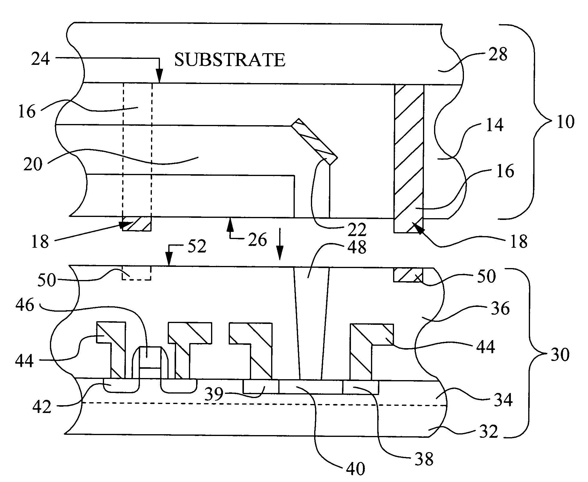
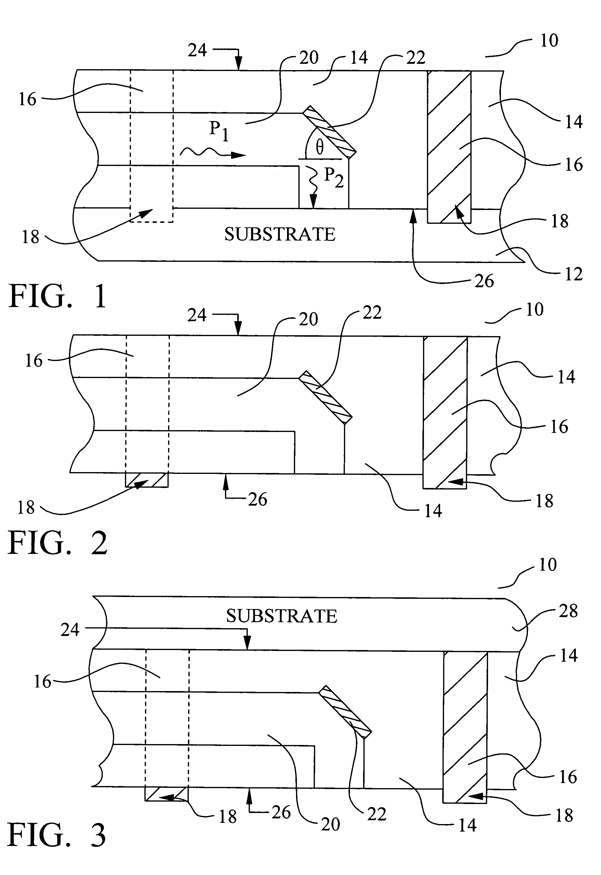
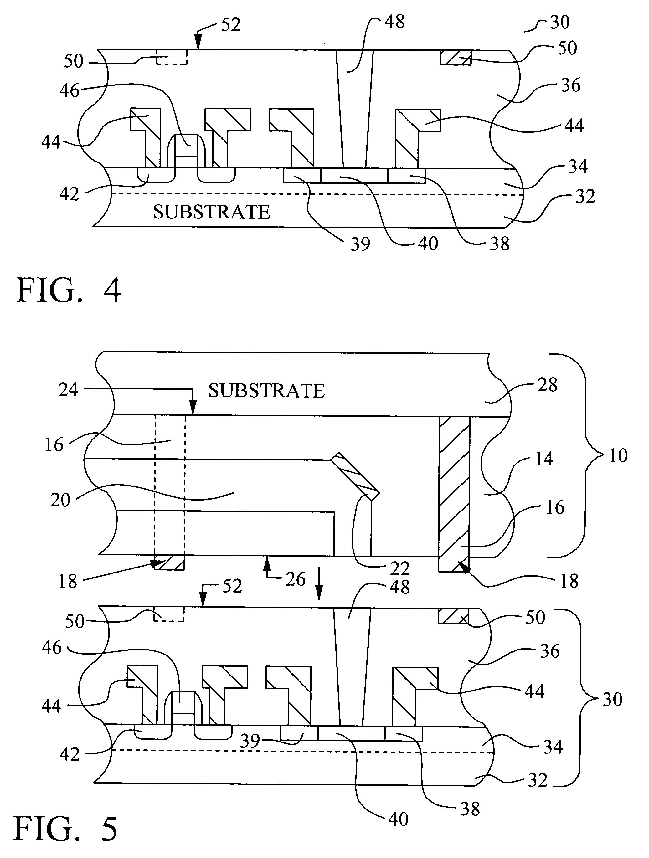
[0029]The preferred embodiments of the present invention disclose methods to form hybrid, optical and electronic integrated circuit devices. An embodiment of the present invention relates to the integration of an optical wafer, or chip, with built-in optical devices such as waveguides or light emitter diodes, with an electronic wafer, or chip, with built-in electronic devices, such as transistors or photodetectors. A wafer bonding process uses thermal diffusion to bond metal to metal and to thereby bond together the optical and electronic substrates. A method to form optical waveguides with embedded mirrors is also disclosed. It should be clear to those experienced in the art that the present invention can be applied and extended without deviating from the scope of the present invention.

[0030]Referring now to FIGS. 1 through 6, a first preferred embodiment of the present invention is illustrated. Several important features of the present invention are shown and discussed below. More...


PUM


Abstract

A new method to form a VLSI-photonic heterogeneous system device is achieved. The method comprises providing an optical substrate comprising at least one passive optical component formed therein. An electronic substrate is provided comprising at least one active electronic component formed therein. A plurality of metal pillars are formed through the optical substrate and protruding out a first surface of the optical substrate. A plurality of metal pads are formed on a first surface of the electronic substrate. The optical substrate and the electronic substrate are bonding together by a method further comprising aligning the first surfaces of the optical and electronic substrates such that the protruding metal pillars contact the metal pads. The optical and electronic substrates are then thermally treated such that the metal pillars bond to the metal pads.

Description

[0001]This application claims priority to U.S. Provisional Application Ser. No. 60 / 501,669 filed on Sep. 10, 2003, herein incorporated by reference.BACKGROUND OF THE INVENTION[0002](1) Field of the Invention[0003]The invention relates to the integration of optical and electronic chips, and, more particularly, to a method to form a hybrid, VLSI-photonic integrated circuit using wafer bonding.[0004](2) Description of the Prior Art[0005]In optical modules for access and metropolitan networking, several requirements are anticipated in the future. In particular, it is anticipated that transmitters, fibers, regenerators, switches, and receivers will become highly integrated components at distribution nodes. Very low cost, plug-and-play systems, such as transmitters and receivers, optical network units (ONU), and optical termination lines (OTL) operating at frequencies in excess of 10 Gigabits / second will be required.[0006]The current state of the art in heterogeneous integration is the si...

Claims


Application Information

Patent Timeline
Patent Type & Authority Patents(United States)
IPC IPC(8): G02B6/12G02B6/43H01L21/50
CPCG02B6/12G02B6/12004G02B6/43G02B2006/12104
Inventor DOAN, MY THE
Owner AGENCY FOR SCI TECH & RES
Why Eureka
Try Eureka