Method for transfer of thin-film of silicon carbide via implantation and wafer bonding

a technology of silicon carbide and thin film, which is applied in the direction of semiconductor/solid-state device manufacturing, basic electric elements, electric apparatus, etc., can solve the problems of not being able to use electronic device applications, not being able to transfer thin films of sufficient quality for device applications, and deactivating or passively transferring carriers

Inactive Publication Date: 2002-03-12
LOCKHEED MARTIN ENERGY SYST INC +1
View PDF10 Cites 53 Cited by
  • Summary
  • Abstract
  • Description
  • Claims
  • Application Information

AI Technical Summary

Problems solved by technology

While the process described above has been successfully applied to silicon technology to produce high quality, silicon-on-insulator wafers, it has not been proven successful for the transfer of thin films of SiC of sufficient quality for device applications.
A significant problem has been associated with the implantation step.
The high resistivity of the implanted SiC material persists even after high temperature annealing at approxi

Method used


Image

  • Method for transfer of thin-film of silicon carbide via implantation and wafer bonding
  • Method for transfer of thin-film of silicon carbide via implantation and wafer bonding
  • Method for transfer of thin-film of silicon carbide via implantation and wafer bonding

Examples


first embodiment

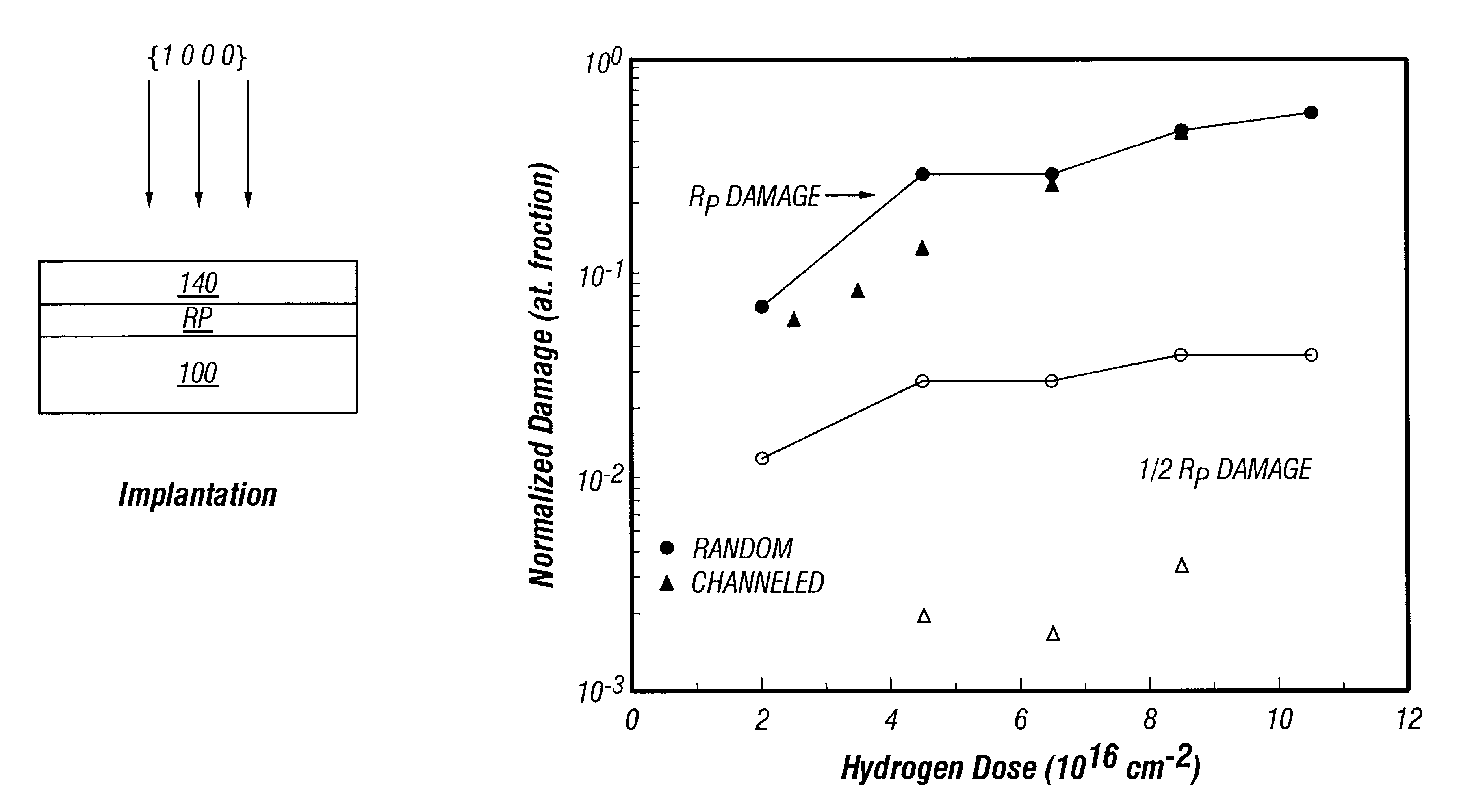
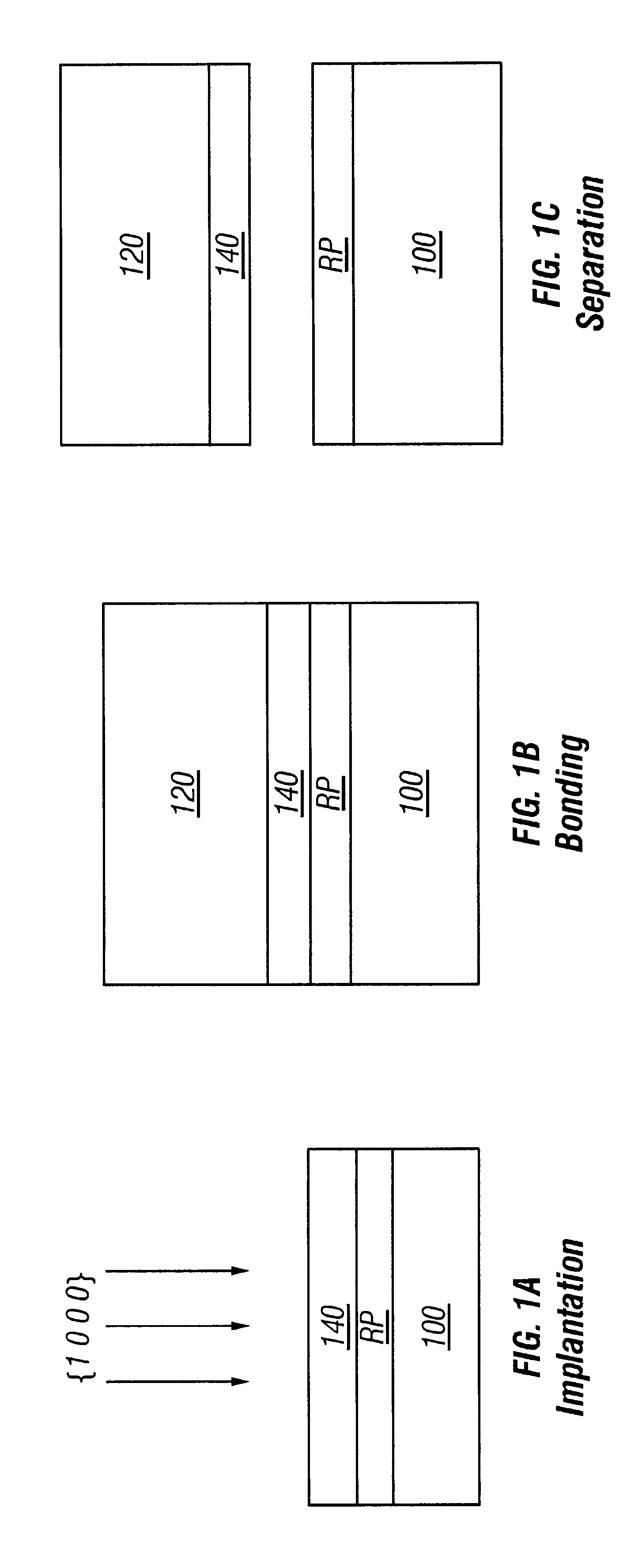
A first embodiment of the invention is based on the use of channeled light-ion implantation to effect the thin-film transfer process. This embodiment is depicted schematically in FIGS. 1A-1C.

FIG. 1A depicts light-ion implantation of a bulk SiC single-crystal 100 along the {1 0 0 0} direction. The light-ions can include hydrogen ions. A thin-film 140 is defined above a strained region R.sub.p. Substrate 100 may include an epitaxial silicon carbide film with controlled impurity doping. Thin-film 140 is defined above the strained region Rp, both of which are included in the silicon carbide crystal 100.

FIG. 1B illustrates the bulk SiC single-crystal 100 being bonded to a target wafer 120. To ensure good bonding, the single-crystal 100 and / or the target wafer 120 can be oxidized or deposited with a thin-film of silicon oxide. Any oxide coating on the single-crystal 100 should be applied after light-ion implantation to avoid scattering of the ions during channeling.

FIG. 1C depicts separat...

second embodiment

A second embodiment of the invention is based on high-temperature processing of the wafers. If the implantation is done at high-temperature (e.g. 600.degree. C.), a substantial reduction of the critical dose, as well as ion-induced damage occurs compared to room-temperature (e.g. 20.degree. C.) processing.

In the case of SiC, implantation at an elevated temperature of approximately 600.degree. C. reduces the critical dose by nearly a factor of 2, from 4.5.times.10.sup.16 cm.sup.-2 per square at room-temperature to 2.8.times.10.sup.16 cm.sup.-2 per square. The retained fraction of hydrogen in the sample implanted at 600.degree. C. is higher by about a factor of 2 than in room-temperature samples (after cycling 1200.degree. C.). This reduces the amount of hydrogen diffusing within the thin-film so that void formation is suppressed.

Of course the invention is not limited to SiC. Any crystal targets can be used. The crystal targets can be held at approximately 300.degree. C., approximatel...

third embodiment

A third embodiment of the invention is based on a combination of both the first embodiment and the second embodiment (i.e. channeled-ion implantation at elevated temperatures). This allows the use of a lower dose and thus less chance of producing lattice damage. In the case of a silicon carbide crystal, this combination approach further reduces the critical dose to approximately 2.5.times.10.sup.16 cm.sup.-2.

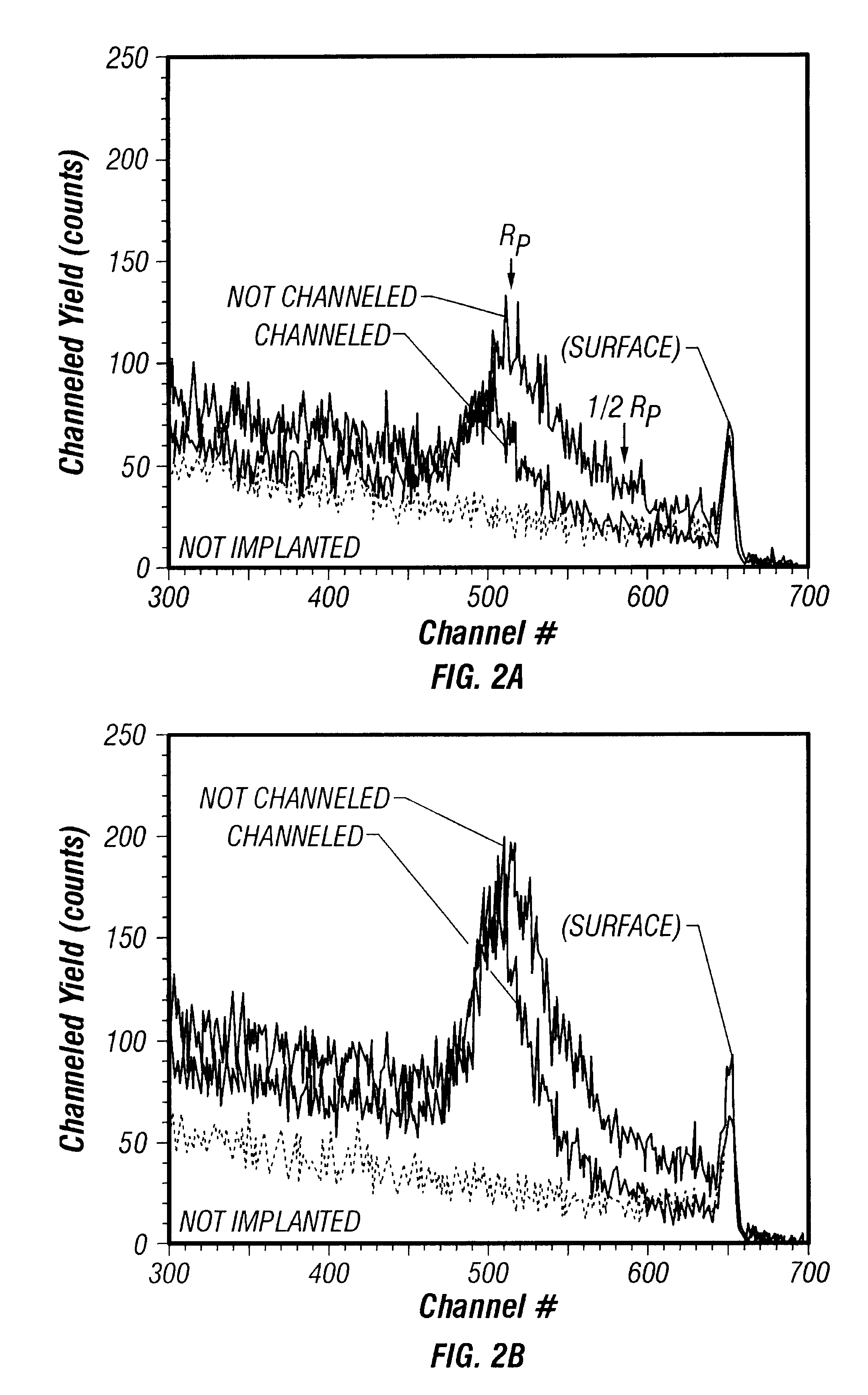
While not being limited to any particular performance indicator or diagnostic identifier, preferred embodiments of the invention can be identified one at a time by testing for the presence of a narrow region of strain (Rp). The test for the presence of narrow Rp can be carried out without undue experimentation by the use of a simple and conventional Rutherford backscattering experiment. Another way to seek embodiments having the attribute of a narrow region of strain is to test for the presence of smooth topography after thin-film transfer.

Practical Applications of the Invention...


PUM


Abstract

Systems and methods are described for transfer of a thin-film via implantation, wafer bonding, and separation. A method for transfer of a thin-film, includes: implanting a source crystal with ions along a crystallographic channel and at a temperature of at least approximately 200° C. to i) form a strained region and ii) define the thin-film; then bonding a surface of the thin-film to a target wafer; and then separating a) the target wafer and the thin-film from b) a remainder of the source crystal along the strained region. The systems and methods provide advantages because the electrical carriers in the crystal, and consequently the thin-film, are not deactivated and the quality of the transferred thin-film is improved.

Description

1. Field of the InventionThe invention relates generally to the field of blistering to form thin-films. The thickness of the film is determined by the penetration depth of the implanted ions which is nominally less than several microns. More particularly, the invention relates to an efficient method for transfer of thin-films of SiC utilizing lattice oriented implantation and wafer bonding.2. Discussion of the Related ArtThin films of silicon carbide can be cleaved or delaminated from a bulk crystal and transferred to another substrate utilizing implantation and wafer bonding. This process involves implantation of hydrogen into a bulk crystal to produce an implanted layer having a highly damaged (and strained) region near the mean range of the ions. This region can be denoted R.sub.p. The bulk crystal (or the source substrate) is then bonded to another substrate, hereafter referred to as the target, and the bonded pair are then thermally cycled causing the implanted layer to delamin...

Claims


Application Information

Patent Timeline
IPC IPC(8): H01L21/762H01L21/70
CPCH01L21/76254
Inventor HOLLAND, ORIN WAYNETHOMAS, DARRELL KEITHGREGORY, RICHARD BAYNEWILSON, SYD ROBERTWETTEROTH, THOMAS ALLEN
Owner LOCKHEED MARTIN ENERGY SYST INC
Why Eureka
Try Eureka