Method for producing nitride semiconductor, crystal growth rate increasing agent, single crystal nitride, wafer and device

a technology of nitride semiconductor and crystal growth rate increasing agent, which is applied in the direction of crystal growth process, polycrystalline material growth, magnesium halide, etc., can solve the problem of difficult to uniformly expose raw materials in a large area, large-diameter m plane can be hardly grown, and large-diameter crystals cannot be produced in the technique field, so as to achieve high performance and significant increase in the growth rate of nitride semiconductor

Inactive Publication Date: 2010-04-29
MITSUBISHI CHEM CORP +1
View PDF8 Cites 287 Cited by
  • Summary
  • Abstract
  • Description
  • Claims
  • Application Information

AI Technical Summary

Benefits of technology

[0060]According to the production method of the present invention, a nitride semiconductor having a large-diameter C plane or a nitride semiconductor thick in the m-axis direction can be efficiently and simply produced. Also, according to the growth rate increasing agent of the present invention, the ...

Problems solved by technology

Also, in the vapor phase epitaxial method, a large-diameter crystal cannot be produced in view of technique, because it is difficult to uniformly expose a raw material in a large area.
However, in the heteroepitaxial growth method on a substrate such as sapphire or silicon carbide by the MOCVD method or the like, which is being performed at present, a high-quality and large-diameter M plane can be hardly grown.
However, in these publications, ...

Method used


Image

  • Method for producing nitride semiconductor, crystal growth rate increasing agent, single crystal nitride, wafer and device
  • Method for producing nitride semiconductor, crystal growth rate increasing agent, single crystal nitride, wafer and device

Examples


example 1

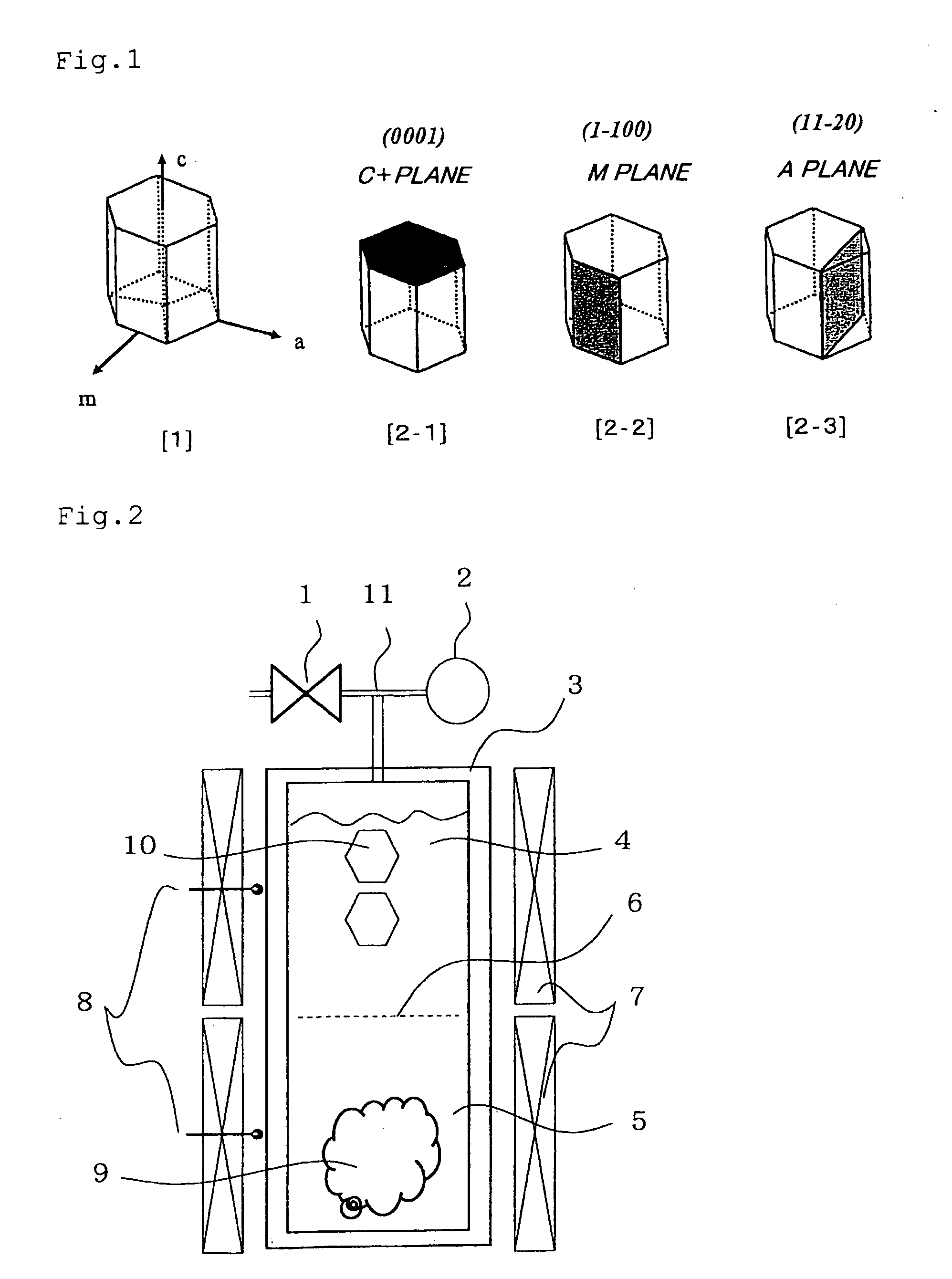
[0113]Crystal growth was performed using an apparatus shown in FIG. 2.

[0114]Using a platinum-lined autoclave 3 (made of Inconel 625, about 30 ml) with the inside dimension having a diameter of 16 mm and a length of 160 mm, 7.4 g of HVPE-grown GaN as a raw material 9 was placed in a raw material filling part 5 of the autoclave, and 1.57 g of fully dried powder NH4Cl (purity: 99.99%) as a mineralizer was further filled thereon.

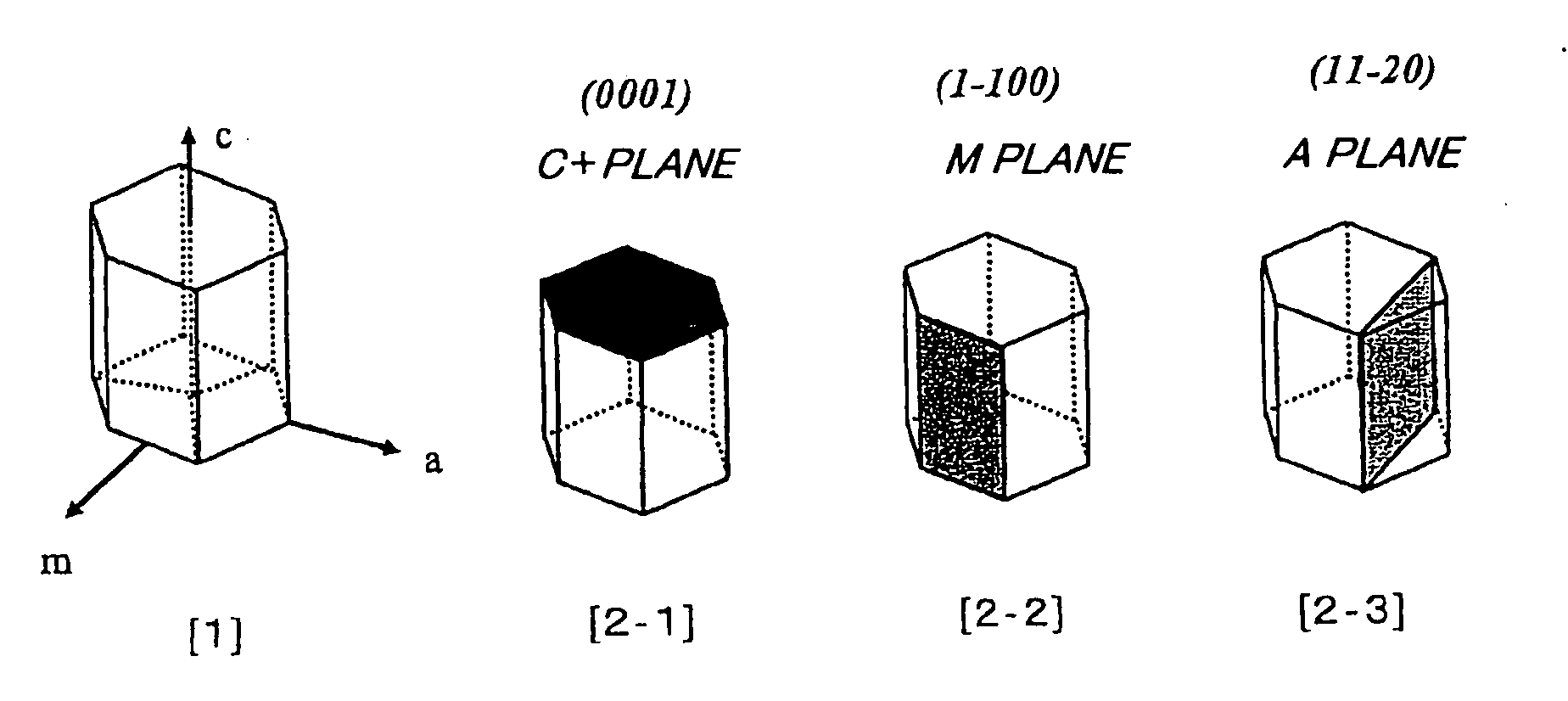
[0115]A baffle plate 6 was then set in the position at 80 mm from the bottom, a GaN seed was disposed in the crystal growth part 4 above the plate and after quickly closing an autoclave cover equipped with a valve, the autoclave 3 was weighed. The GaN seed 10 used here is a seed having a 5 mm-square C plane with the thickness in the c-axis direction being 500 μm, in which one side face is an M plane produced by cleavage. Subsequently, a channel 11 was operated to communicate with a vacuum pump through a valve 1 attached to the autoclave, and the inside of the au...


PUM


Abstract

A method for producing a nitride semiconductor, comprising controlling temperature and pressure in a autoclave containing a seed having a hexagonal crystal structure, a nitrogen element-containing solvent, a raw material substance containing a metal element of Group 13 of the Periodic Table, and a mineralizer so as to put said solvent into a supercritical state and/or a subcritical state and thereby ammonothermally grow a nitride semiconductor crystal on the surface of said seed, wherein the crystal growth rate in the m-axis direction on said seed is 1.5 times or more the crystal growth rate in the c-axis direction on said seed. By the method, a nitride semiconductor having a large-diameter C plane or a nitride semiconductor thick in the m-axis direction can be efficiently and simply produced.

Description

TECHNICAL FIELD[0001]The present invention relates to a production method of a nitride semiconductor, where the crystal growth of a nitride semiconductor on a seed is performed by using a solvent in a supercritical state and / or a subcritical state together with a raw material substance and a mineralizer, and a crystal growth rate increasing agent for use in the production method. The present invention also relates to a single crystal nitride produced by the method, a wafer and a device.BACKGROUND ART[0002]A nitride semiconductor as typified by gallium nitride (GaN) is useful as a substance applied to a light-emitting device such as light-emitting diode and laser diode or to a high-frequency and / or high-output electronic device such as HEMT and HBT. Particularly, in usage for an electronic device expected to expand its market in the future, the device size is larger than that of a light-emitting device and in view of productivity, formation of a large-diameter wafer is more keenly de...

Claims


Application Information

Patent Timeline
IPC IPC(8): C30B9/00C01F11/20C01B21/06
CPCC30B7/10C30B29/406C30B29/403C30B29/38H01L21/20
Inventor KAWABATA, SHINICHIROITOH, HIROHISAEHRENTRAUT, DIRKKAGAMITANI, YUJIYOSHIKAWA, AKIRAFUKUDA, TSUGUO
Owner MITSUBISHI CHEM CORP
Why Eureka
Try Eureka