Semiconductor processing

a technology of semiconductors and semiconductors, applied in the field of semiconductor processing, can solve the problems of large bulky and large volume of the static concentrator system made with such cells, and achieve the effect of increasing the usable surface area

Inactive Publication Date: 2005-12-08
AUSTRALIEN NAT UNIV
View PDF99 Cites 48 Cited by
  • Summary
  • Abstract
  • Description
  • Claims
  • Application Information

AI Technical Summary

Benefits of technology

[0004] In accordance with a first embodiment of the present invention, there is provided a method for increasing the usable surface area of a semiconductor wafer having a substantially planar surface and a thickness dimension at right angles to said substantially planar surface, said method including the steps of selecting a strip thickness for division of the wafer into a plurality of strips, selecting a technique for cutting the wafer into said strips at an angle to said substantially planar surface, in which the combined strip thickness and width of wafer removed by the cutting is less than the thickness of the wafer, cutting the wafer into strips using the selected technique and separating the strips from each other.
[0026] In a further form of the methods of the first to third embodiments of the invention, at least one interconnecting portion is formed in or on the wafer, which connects adjoining strips to each other to maintain a relatively constant gap between the strips. Usually, in this form of the methods of the invention, there are a plurality of interconnecting strips. Conveniently, the interconnecting strips are spaced apart at regular intervals along the length of the strips. The inclusion of such interconnecting portions allows processing steps such as diffusions and oxidations to be carried out in a reliable and repeatable manner, resulting in predictable diffusion profiles and oxide thicknesses down the sides of the slots. The interconnecting portions suitably take the form of one or more strips of the semiconductor material formed at least partly across one or both main surfaces thereof, perpendicular or oblique to, and usually substantially perpendicular to, the strips which are defined by the plurality of slots.
[0030] Advantageously, solar cells made by a process which includes a method in accordance with the present invention may be arranged with gaps between adjacent cells and used with an optical concentrator to increase the effective solar cell area.
[0037] In the process of this embodiment, by “substantially unetched” is meant that the etching is carried out under conditions in which the semiconductor material is etched in the vicinity of the apertures in the protective substance, but sufficient of the protective substance remains on the surface of the semiconductor material at the end of the etching to prevent the semiconductor material from being etched in regions other than in the vicinity of the apertures.

Problems solved by technology

Standard solar cells of the prior art, made from wafers, are typically 10×10 cm2 or larger, and therefore static concentrator systems made with such cells are large and bulky.

Method used


Image

  • Semiconductor processing
  • Semiconductor processing
  • Semiconductor processing

Examples


example 1

Fabrication of Solar Cell

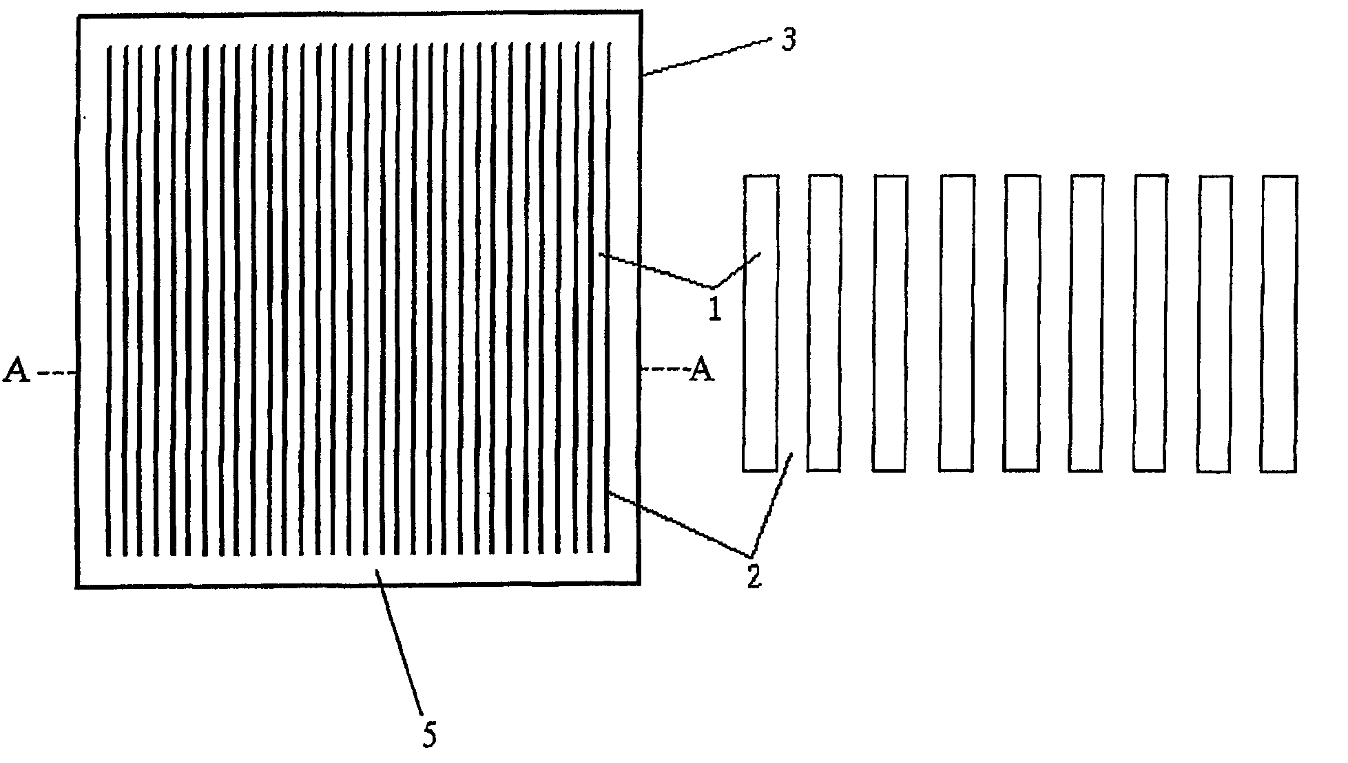
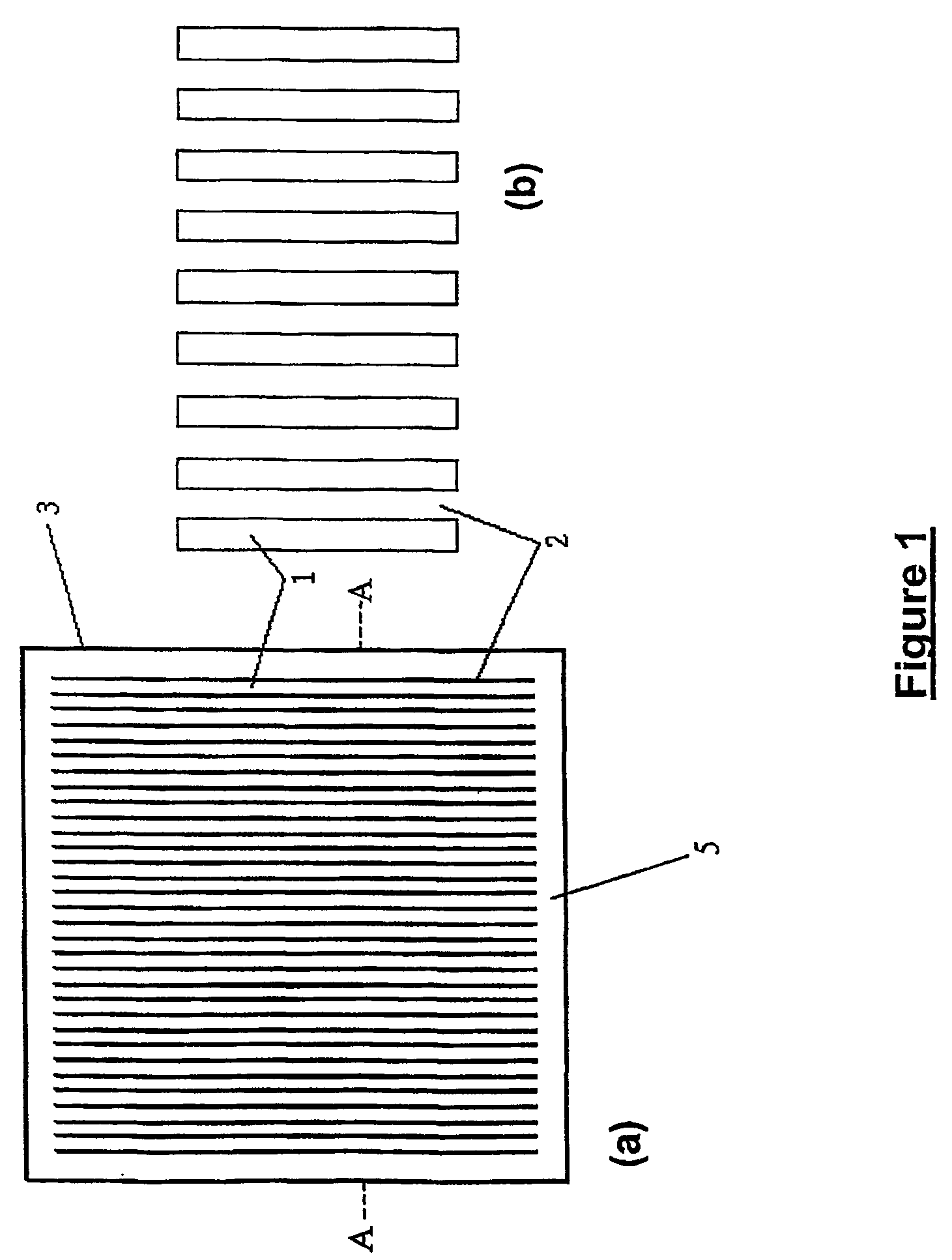
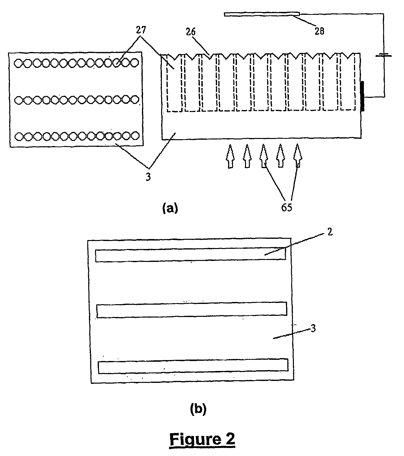
[0099] Solar cells have been fabricated as follows. 0.5 Ohm-cm, boron doped float-zoned wafers, 100 mm in diameter and 0.8 mm thick, were used as the starting material. The wafers were etched to remove any surface damage. A phosphorus diffusion was made into one side of the wafer (the top side) to a sheet resistance of approximately 50 ohm / square, followed by a boron diffusion into the rear side to about 50 ohm / square. A 100 nm thick oxide was grown on both surfaces, followed by deposition of 50 nm of silicon nitride. Cuts were made into the wafers from the top side using a dicing saw, with the cuts extending to within approximately 50 microns of the rear surface, to create silicon strips. The wafers were then given an etch in potassium hydroxide solution to remove any damage resulting from the cutting process. A phosphorus diffusion was then made into the grooves to about 100 ohm / square. An oxide was grown on the sidewalls of the strips to a thickness of 2...

example 2

Texturing polished silicon surface to decrease reflectivity

[0101] A silicon nitride layer approximately 2 nm thick was deposited at 750° C. on a polished silicon wafer of (111) orientation, using low pressure chemical vapour deposition. A sample was cut out of the wafer and etched in a solution of 1:50 hydrofluoric acid:nitric acid for 150 seconds at 0° C. The sample was encapsulated behind 1 mm thick low iron glass using silicone and its reflectance was measured using a spectrophotometer with an integrating sphere. The sample had a reflectivity of 11% at 900 nm, while a polished encapsulated silicon reference wafer had a reflectivity of 24% and a sample of (100) oriented silicon textured with inverted pyramids had a reflectivity of 8% at the same wavelength. These results indicate that the texturing process is very effective at reducing reflection from the silicon surface. The results also indicate that the texture is likely to be very effective at confining light within the silic...


PUM

PropertyMeasurementUnit
angleaaaaaaaaaa
diameteraaaaaaaaaa
diameteraaaaaaaaaa

Abstract

The invention provides a method for increasing the usable surface area of a semiconductor wafer having a substantially planar surface and a thickness dimension at right angles to said substantially planar surface, the method including the steps of selecting a strip thickness for division of the wafer into a plurality of strips, selecting a technique for cutting the wafer into the strips at an angle to the substantially planar surface, in which the combined strip thickness and width of wafer removed by the cutting is less than the thickness of the wafer, cutting the wafer into strips using the selected technique and separating the strips from each other.

Description

STATEMENT OF RELATED APPLICATIONS [0001] This application is a continuation of U.S. application Ser. No. 10 / 432,936, filed May 28, 2003, which is a 371 U.S. National Phase application claiming priority to PCT / AU01 / 01546, filed Nov. 29, 2001, which is based on Australian provisional application PRI748, filed Nov. 29, 2000.FIELD OF THE INVENTION [0002] The present invention relates to semiconductor processing, and in particular to methods for processing a semiconductor wafer to increase the useable planar surface area, to a method for fabricating solar cells and to a process for decreasing the reflectivity of a semiconductor surface. BACKGROUND OF THE INVENTION [0003] In most areas of semiconductor processing, the cost of the starting substrate wafer is small compared to the value of the final, processed wafer. However, this is not always the case. For example, the photovoltaic solar cell industry is extremely cost sensitive, and the cost of a starting silicon wafer is typically nearl...

Claims


Application Information

Patent Timeline
Patent Type & Authority Applications(United States)
IPC IPC(8): B23KB23K101/40H01LH01L21/00H01L21/306H01L21/301H01L21/46H01L21/4763H01L21/50H01L21/78H01L31/0236H01L31/05H01L31/052H01L31/054H01L31/068H01L31/18
CPCH01L31/068H01L31/18H01L31/1804H01L31/1876Y02E10/52Y02E10/547H01L31/035281H01L31/0504Y02P70/521H01L31/0547Y02P70/50H01L21/302
Inventor WEBER, KLAUS JOHANNESBLAKERS, ANDREW WILLIAM
Owner AUSTRALIEN NAT UNIV
Why Eureka
Try Eureka