Self-aligned selective hemispherical grain deposition process and structure for enhanced capacitance trench capacitor

a trench capacitor and selective hemispherical grain technology, applied in the direction of basic electric elements, electrical equipment, semiconductor devices, etc., to achieve the effect of increasing the surface area availabl

Inactive Publication Date: 2006-09-05
GLOBALFOUNDRIES INC
View PDF12 Cites 4 Cited by
  • Summary
  • Abstract
  • Description
  • Claims
  • Application Information

AI Technical Summary

Benefits of technology

[0004]The present invention provides a way of increasing the amount of surface area available between plates of a trench storage capacitor by forming an uneven plate surface by deposited hemispherical silicon grains, and then forming the capacitor dielectric and a conductor on the other side of the dielectric.

Problems solved by technology

However, the inability to shrink cell voltages and currents as rapidly as the cell area means that proportionally more capacitance is demanded from the storage capacitor per unit of area defined by the initial etch of the trench at critical dimension.

Method used


Image

  • Self-aligned selective hemispherical grain deposition process and structure for enhanced capacitance trench capacitor

Examples


Embodiment Construction

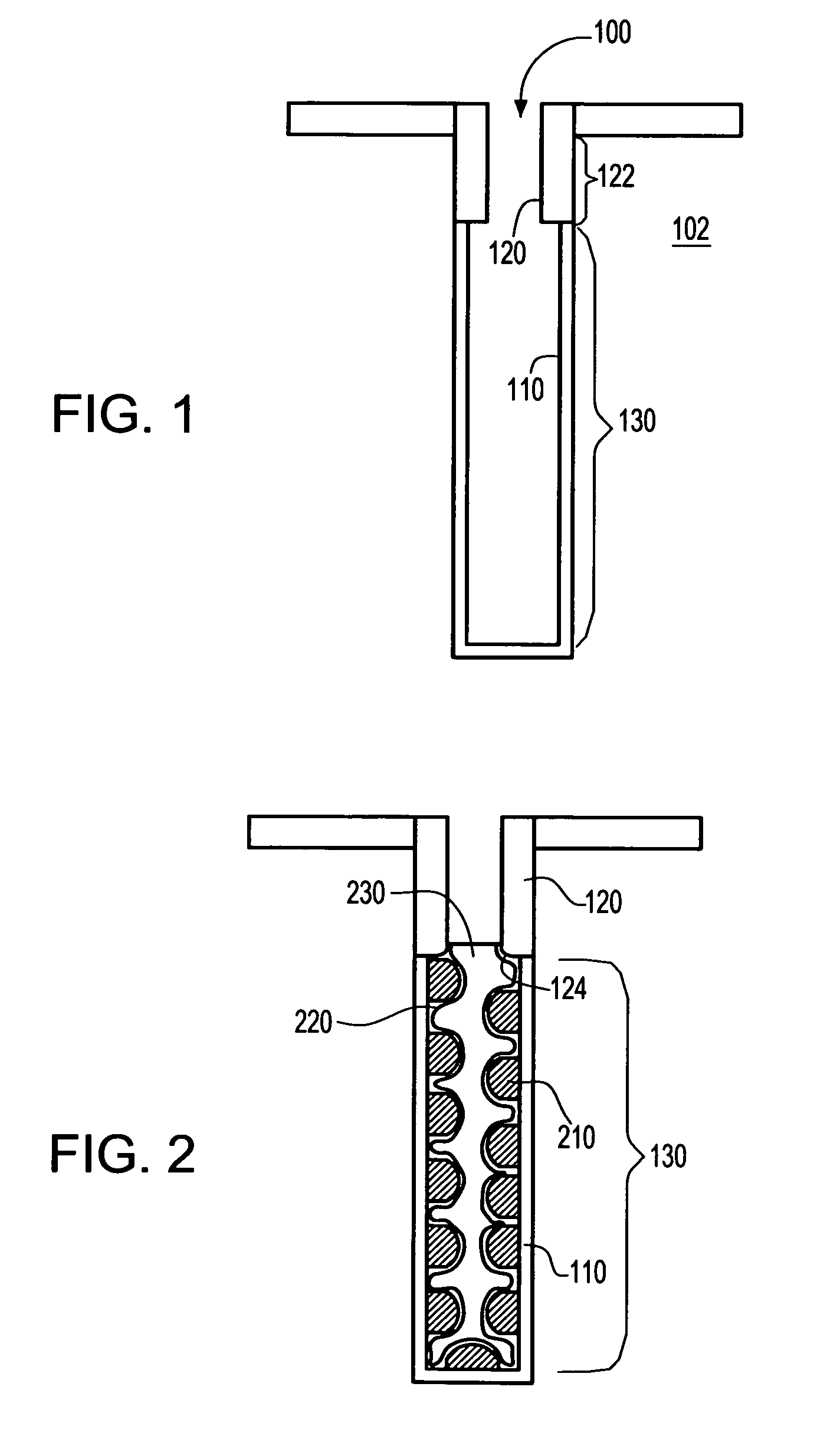
[0008]One way to increase the surface area available as the dielectric interface between plates of a capacitor is to provide a plate having an uneven surface, and then depositing a compatible dielectric material over it, such that the dielectric material generally assumes the unevenness of the plate surface below that.

[0009]Depositing hemispherical silicon grains (hereinafter, “HSG”) onto sidewalls of a deep trench may be a way to create an uneven surface, and thereby increase the surface area of a trench capacitor. However, at small groundrules of 110 nanometers and below, HSG deposition in the context of existing trench capacitor processing appears problematic. For example, depositing HSG into deep trenches after forming the isolation collar could fail due to HSG adhering to the collar and pinching off the trench, causing few grains to be deposited in the bottom of the trench. Therefore, it becomes imperative to use a selective HSG process such that grains are deposited in a lower...


PUM


Abstract

As disclosed herein, a method is provided, in an integrated circuit, for forming an enhanced capacitance trench capacitor. The method includes forming a trench in a semiconductor substrate and forming an isolation collar on a sidewall of the trench. The collar has at least an exposed layer of oxide and occupies only a “collar” portion of the sidewall, while a “capacitor” portion of the sidewall is free of the collar. A seeding layer is then selectively deposited on the capacitor portion of the sidewall. Then, hemispherical silicon grains are deposited on the seeding layer on the capacitor portion of the sidewall. A dielectric material is deposited, and then a conductor material, in that order, over the hemispherical silicon grains on the capacitor portion of the sidewall.

Description

FIELD OF THE INVENTION[0001]The invention relates to a semiconductor processing method and structure, and more particularly to a integrated circuit fabrication process and structure for capacitance enhancement of a trench capacitor structure, such as useful in a dynamic random access memory (DRAM), among others.BACKGROUND OF THE INVENTION[0002]In a dynamic random access memory (DRAM), a plurality of memory cells are formed in a matrix manner on a substrate. Each memory cell in a DRAM device is constructed by at least one transistor and at least one storage capacitor. Commonly, either trench capacitor or stacked cells are used. The trenched structure is advantageous to the stacked structure in situations where the surface flatness of the device is of great importance. While trench capacitors are mostly used as storage capacitors in DRAMS, such structures are also used in some integrated circuits as general use capacitors, for example for decoupling purposes.[0003]In DRAMs, as well as...

Claims


Application Information

Patent Timeline
Patent Type & Authority Patents(United States)
IPC IPC(8): H01L21/20H01L21/334H01L21/8242H01L29/94
CPCH01L27/1087H01L29/945H01L29/66181H10B12/0387
Inventor SETTLEMYER, JR., KENNETH T.WRSCHKA, PORSHIA SHANE
Owner GLOBALFOUNDRIES INC
Why Eureka
Try Eureka