Method of fabrication of a micro-channel based integrated sensor for chemical and biological materials

a micro-channel and biological sensor technology, applied in microstructural technology, microstructural devices, liquid/fluent solid measurement, etc., can solve the problems of limited specificity of metal coatings, inability to detect chemical and biological materials, and increase size and manufacturing costs. , to achieve the effect of enhancing the selectivity of sensors

Inactive Publication Date: 2005-08-23
HRL LAB
View PDF6 Cites 51 Cited by
  • Summary
  • Abstract
  • Description
  • Claims
  • Application Information

AI Technical Summary

Benefits of technology

[0020]The present invention describes a new method for simultaneously functionalizing or “activating” MEMS-based chemical or biological sensors with a variety of molecules for enhancing the selectivity of the sensor. This functionalization can occur on-chip using vapor phase deposition and novel microchannel-based distribution from the edge of the wafer.
[0021]Each sensor array on chip can be functionalized in parallel with different molecules before wafer dicing. This reduces the labor required to functionalize each sensor array independently. Wafer bonding and dry plasma etching are utilized for fabrication and provide a lithographic process in which a gold seed layer is coated on the individual cantilevers before functionalization.
[0022]Finally, a novel backside etching procedure is described that releases all the sensors on a wafer while preventing damage to the cantilevers or their coatings.
[0023]The purpose of this invention is threefold. First, it provides a simple and easy method for functionalizing (or coating) multiple sets of closely spaced cantilevers on an entire wafer simultaneously with different molecules. By doing that, it currently solves one of the most difficult tasks in the fabrication of chemical and / or biological MEMS sensors, which is the application of different functionalizing materials on adjacent cantilevers.
[0025]Second, the method allows the integration of electrostatic and capacitive structures on the cantilever wafer for simple actuation and signal detection. By using a unique set of etching and bonding techniques, the cantilevers can be closely spaced to actuation and detection electrodes (within a few micrometers), thus eliminating higher cost, and providing improved detection techniques. These same fabrication techniques also allow a critical gold coating to be lithographically defined on the topside of the cantilevers for later binding to the functionalization layer.
[0026]Finally, it provides a method of dicing the wafer after organic coatings are applied to the cantilevers. This method allows the organic films previously applied to remain intact, while eliminating most of the stress to the devices during mechanical cleaving.

Problems solved by technology

Two limitations of this sensor are that it operates most effectively in a vacuum (requiring substantial instrumentation and making it unsuitable for most biological interactions that are desired) and it is limited in specificity by the reactivity of the metal coating.
Lee's sensor has major drawbacks and disadvantages that also characterize other sensors discussed below.
This prevents the integration of closely packed cantilevers in a sensor and therefore increases the size and the manufacturing costs.
In addition according to the prior art, the individual sensor dies must be functionalized serially which also increases the time and cost of manufacturing.
Thus, these techniques yielded expensive, cumbersome and sluggish sensors.

Method used


Image

  • Method of fabrication of a micro-channel based integrated sensor for chemical and biological materials
  • Method of fabrication of a micro-channel based integrated sensor for chemical and biological materials
  • Method of fabrication of a micro-channel based integrated sensor for chemical and biological materials

Examples


Embodiment Construction

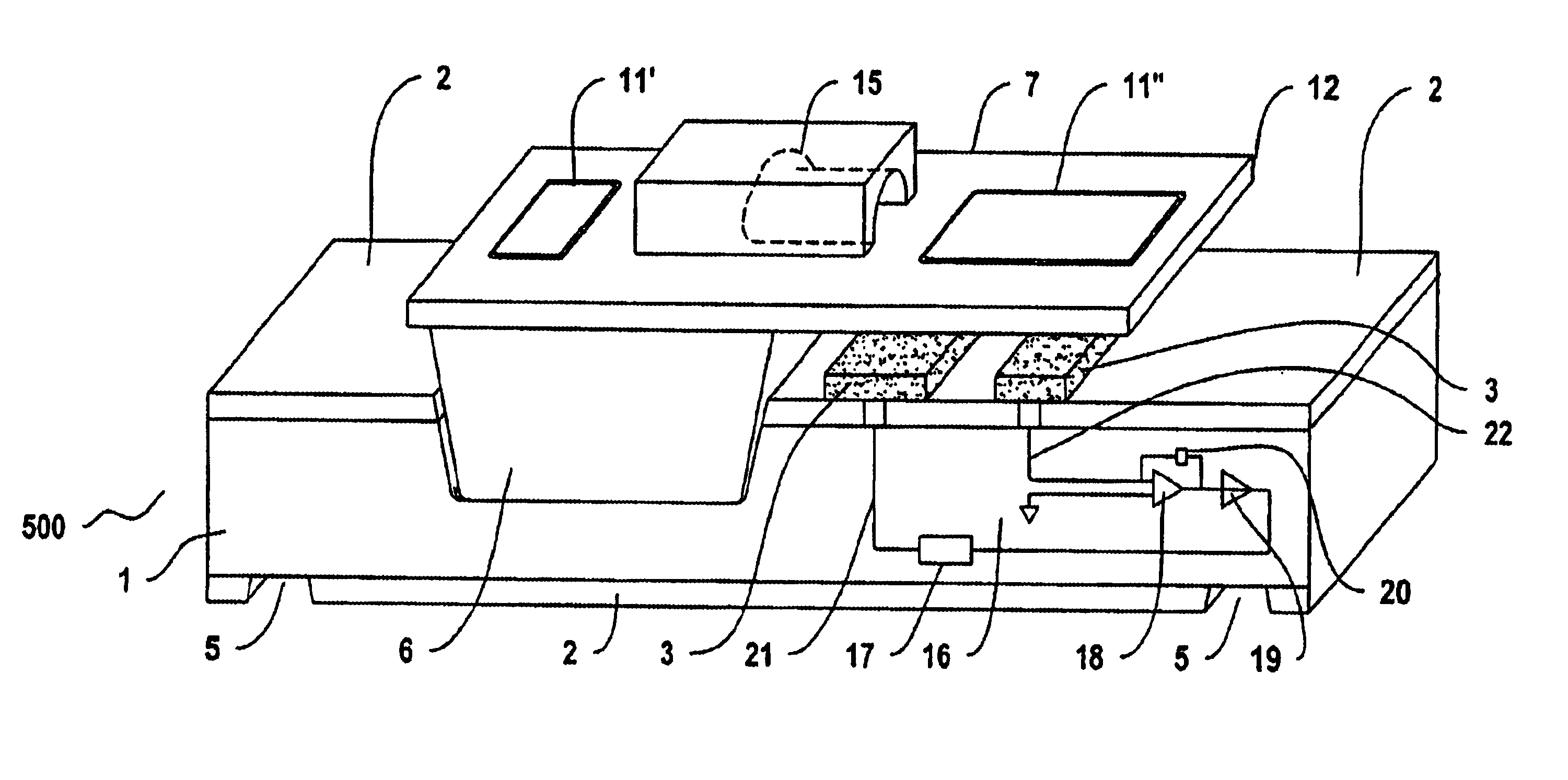
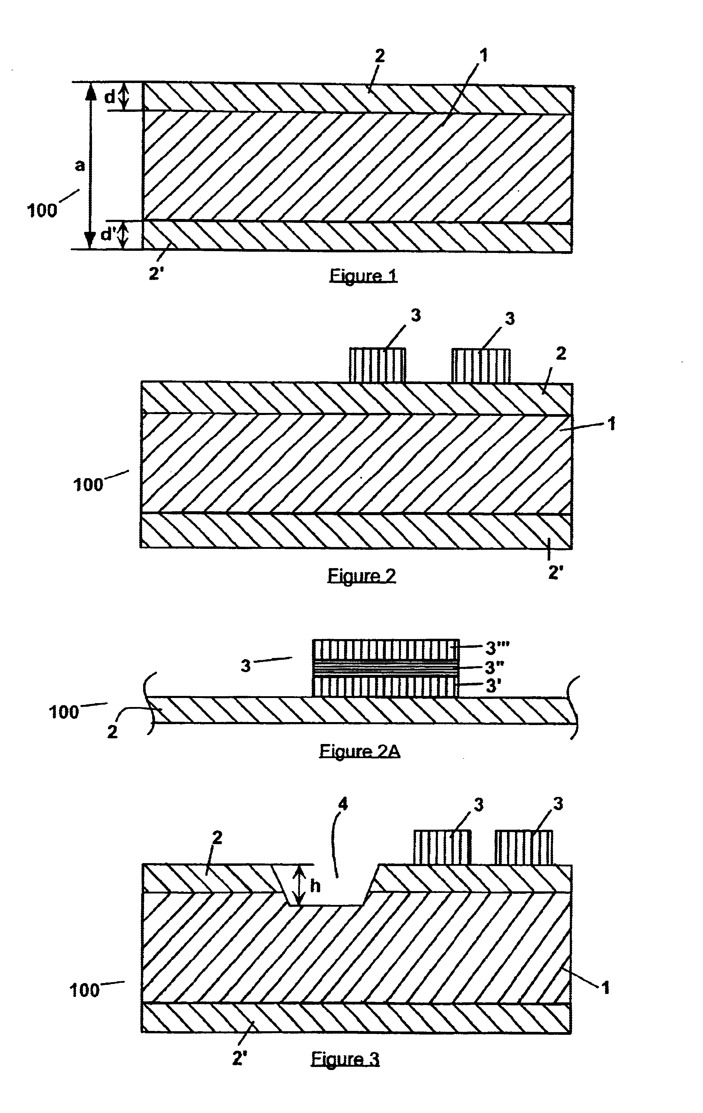
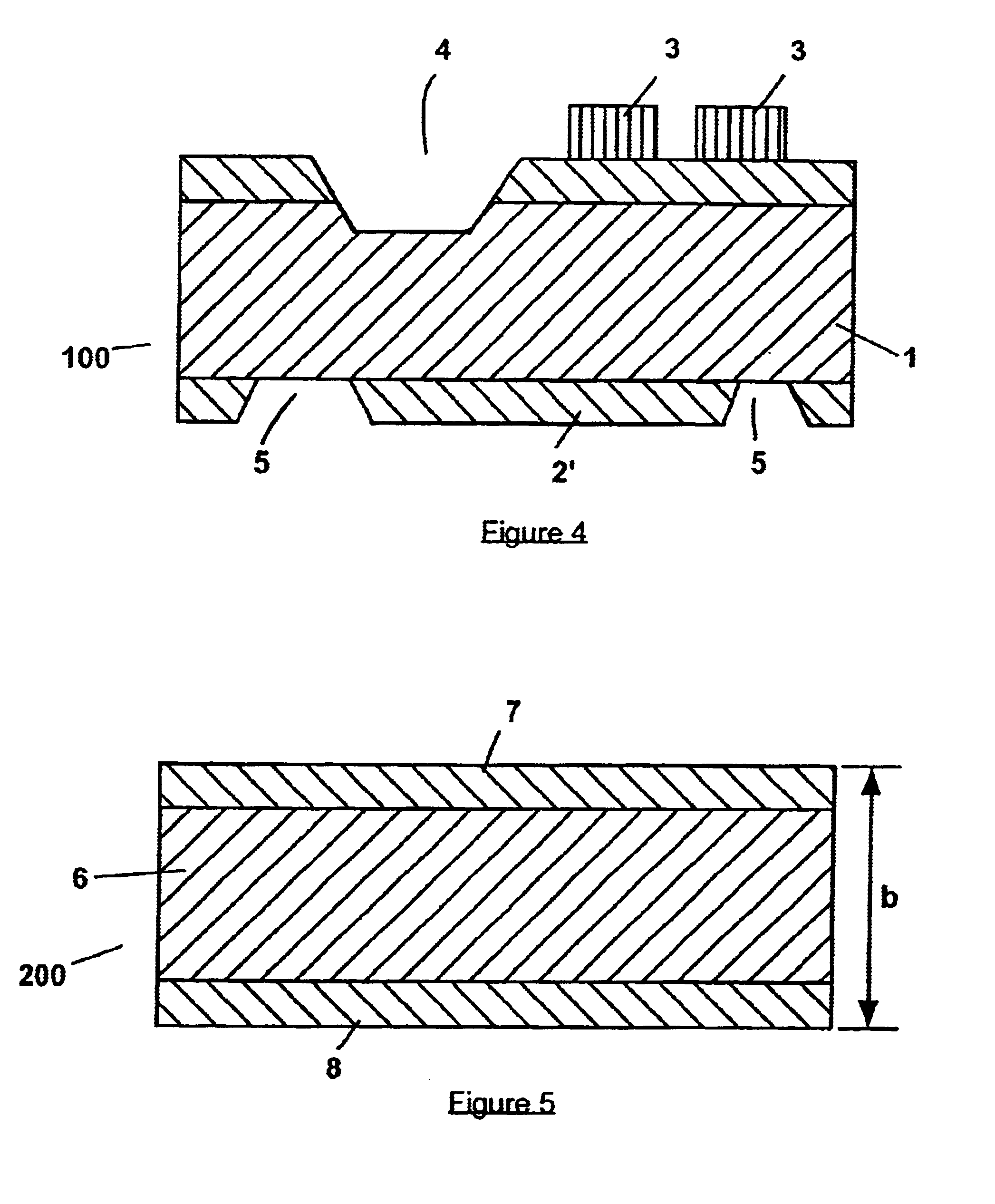
[0048]The sensor which is the subject matter of the present invention preferably comprises three silicon wafers that are mechanically bonded together to produce the final structure. The fabrication process of the sensor is as follows.

[0049]As shown in FIG. 1, the starting wafer or substrate comprises a relatively thick wafer 100. The wafer 100 comprises a layer 1 of a semiconducting material. The semiconducting material is preferably an n-type silicon, and alternatively at least one of a Group III-Group V element. The top side of wafer 100 comprises an insulating material 2, preferably silicon oxide, or silicon nitride, Si3N4, or a combination thereof. The bottom side of wafer 100 comprises a masking material 2′, preferably, Si3N4.

[0050]Total thickness, a, of the wafer 100 is within a range of between about 650 micrometers and about 850 micrometers, preferably about 750 micrometers. Each of the layers of the insulating material 2 and of the masking material 2′ has a thickness, d or ...


PUM

PropertyMeasurementUnit
thicknessaaaaaaaaaa
thicknessaaaaaaaaaa
thicknessaaaaaaaaaa

Abstract

A method for fabricating a sensor for chemical and / or biological materials, comprising steps of providing a wafer comprising a plurality of cantilever assemblies, each of the assemblies comprising a cantilever member and a micro-channel plate bonded to the cantilever member, the micro-channel plate further comprising a micro-channel, functionalizing each of the cantilevers by directing a flow of a plurality of functionalizing materials through the micro-channels, and dicing the wafer into a plurality of the sensors. Each of the cantilever assemblies comprises substrate comprising control and sense electrodes deposited on its top side and scribe marks etched on its back side; a cantilever member comprising a cantilever, a seed layer and a contact pad formed on top side of the cantilever member; and the micro-channel plate comprises a micro-channel housing defining the micro-channel etched through the housing, wherein the back side of the cantilever member is bonded to the substrate and the micro-channel plate is bonded to said top side of the cantilever member. Control electronics are incorporated into the substrate for a completely integrated design.

Description

[0001]This application claims priority under 35 U.S.C. § 119(e) to co-pending U.S. Pat. application Ser. No. 60 / 316,663 (filed on 30 Aug. 2001) entitled “A METHOD OF FABRICATION OF A MICRO-CHANNEL BASED INTEGRATED SENSOR FOR CHEMICAL AND BIOLOGICAL MATERIALS,” the contents of which are hereby expressly incorporated herein in their entirety by this reference.I. BACKGROUND OF THE INVENTION[0002]1. Field of the Invention[0003]This invention relates to the field of sensors for detecting chemical and biological materials. More particularly, it pertains to the novel technique of fabricating integrated micromachined cantilever chemical and / or biological sensors.[0004]2. Description of the Related Art[0005]The need for detection of chemical and / or biological agents in a variety of applications is acute. The rapid detection of very small quantities of harmful molecules, DNA, viruses, etc. using cheap throw-away sensors is particularly important.[0006]A number of methods have been developed w...

Claims


Application Information

Patent Timeline
Patent Type & Authority Patents(United States)
IPC IPC(8): H01L21/00B81B1/00B81B3/00B81C1/00G01N27/00
CPCB81C1/00206B81C1/00904G01N29/036B81B2201/0214B81C2201/0161G01N2291/0256
Inventor KUBENA, RANDALL L
Owner HRL LAB
Why Eureka
Try Eureka