Method of coating water soluble mask for laser scribing and plasma etch

a laser scribing and plasma etching technology, applied in the field of semiconductor wafer dicing, can solve the problems of chip and gouge formation along the severed edge of the dice, inoperable integrated circuit, crack formation and propagation,

Active Publication Date: 2014-01-16
APPLIED MATERIALS INC
View PDF2 Cites 54 Cited by
  • Summary
  • Abstract
  • Description
  • Claims
  • Application Information

AI Technical Summary

Benefits of technology

[0011]In an embodiment, a method of dicing a semiconductor wafer having a plurality of integrated circuits involves forming a hybrid mask above the semiconductor wafer. The hybrid mask is composed of a first water-soluble layer disposed on the integrated circuits, and a second water-soluble layer disposed on the first water-soluble layer. Forming the hybrid mask involves forming the first water-soluble layer with a thickness less than the thickness of the second water-soluble layer, and forming the first water-soluble layer with a viscosity less than the viscosity of the second water-soluble layer. The first water-soluble layer is applied with a first spin-on process and then baked and, subsequently, the second water-soluble layer is applied with a second spin-on process and then baked. The method also involves patterning the hybrid mask with a laser scribing process to provide a patterned hybrid mask with gaps, exposing regions of the semiconductor wafer between the integrated circuits. The method also involve

Problems solved by technology

One problem with either scribing or sawing is that chips and gouges can form along the severed edges of the dice.
In addition, cracks can form and propagate from the edges of the dice into the substrate and render the integrated circuit inoperative.
Chipping and cracking are particularly a problem with scribing because only one side of a square or rectangular die can be scribed in the direction of the crystalline structure.
Consequently, cleaving of the other side of the die results in a jagged separation line.
As a result of the spacing requirements, not as many dice can be formed on a standard sized wafer and wafer real estate that could oth

Method used


Image

  • Method of coating water soluble mask for laser scribing and plasma etch
  • Method of coating water soluble mask for laser scribing and plasma etch
  • Method of coating water soluble mask for laser scribing and plasma etch

Examples


Embodiment Construction

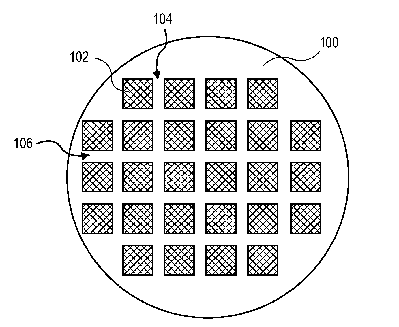
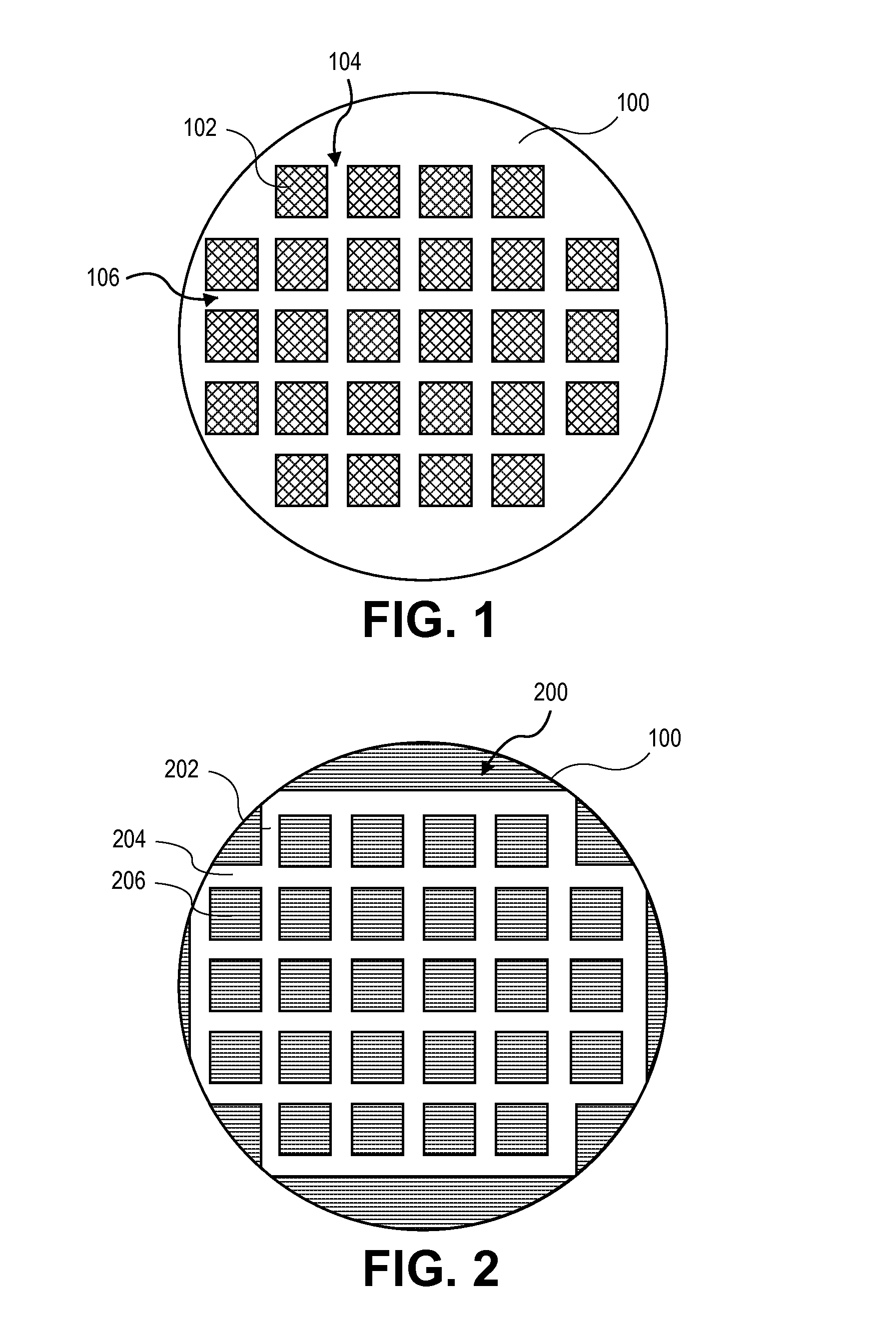
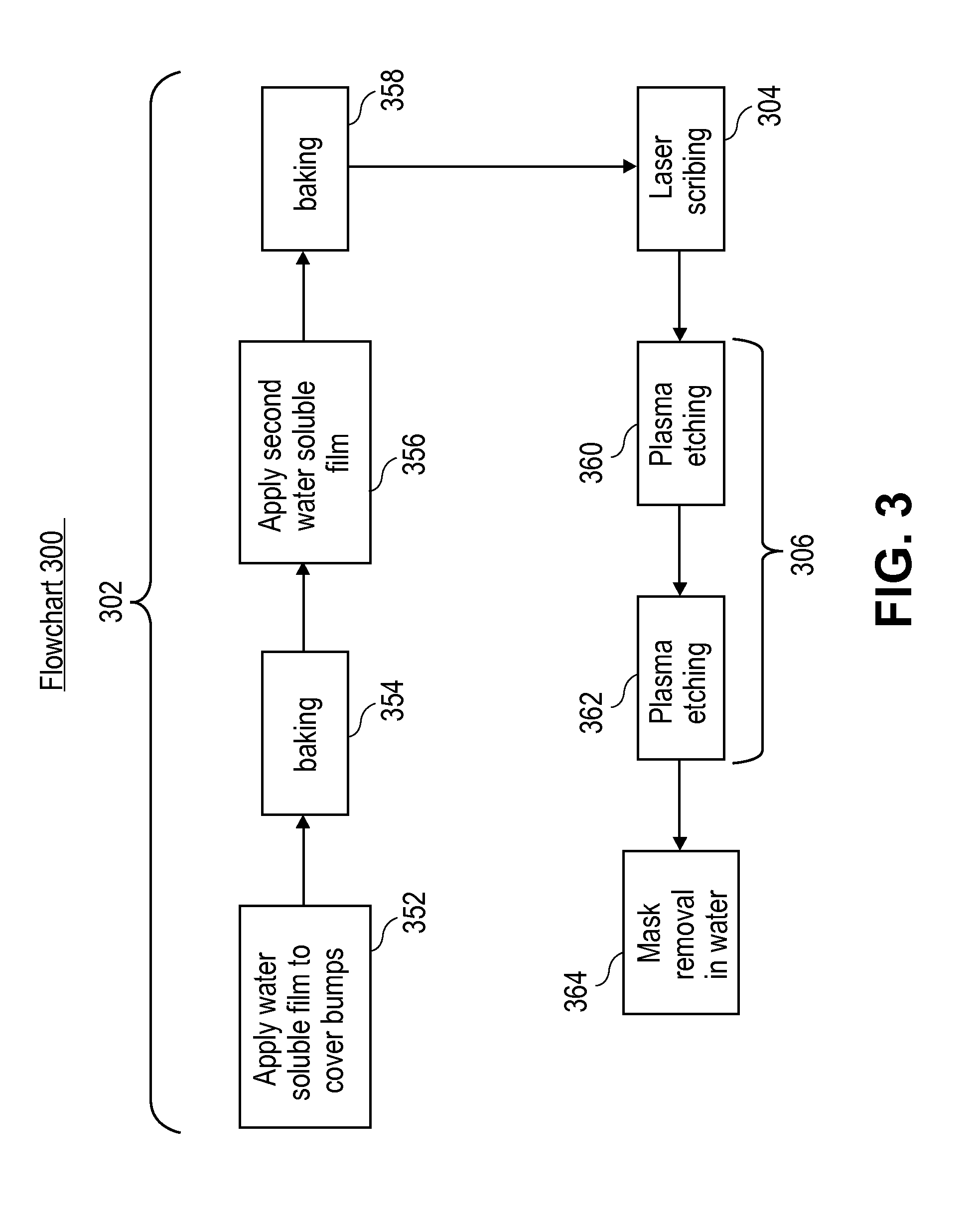
[0027]Methods of dicing semiconductor wafers, each wafer having a plurality of integrated circuits thereon, are described. In the following description, numerous specific details are set forth, such as femtosecond-based laser scribing and plasma etching conditions and material regimes, in order to provide a thorough understanding of embodiments of the present invention. It will be apparent to one skilled in the art that embodiments of the present invention may be practiced without these specific details. In other instances, well-known aspects, such as integrated circuit fabrication, are not described in detail in order to not unnecessarily obscure embodiments of the present invention. Furthermore, it is to be understood that the various embodiments shown in the Figures are illustrative representations and are not necessarily drawn to scale.

[0028]A hybrid wafer or substrate dicing process involving an initial laser scribe and subsequent plasma etch may be implemented for die singulat...


PUM


Abstract

Methods of using a hybrid mask composed of a first water soluble film layer and a second water-soluble layer for wafer dicing using laser scribing and plasma etch described. In an example, a method of dicing a semiconductor wafer having a plurality of integrated circuits involves forming a hybrid mask above the semiconductor wafer. The hybrid mask is composed of a first water-soluble layer disposed on the integrated circuits, and a second water-soluble layer disposed on the first water-soluble layer. The method also involves patterning the hybrid mask with a laser scribing process to provide a patterned hybrid mask with gaps, exposing regions of the semiconductor wafer between the integrated circuits. The method also involves etching the semiconductor wafer through the gaps in the patterned hybrid mask to singulate the integrated circuits.

Description

CROSS-REFERENCE TO RELATED APPLICATIONS[0001]This application claims the benefit of U.S. Provisional Application No. 61 / 671,324, filed Jul. 13, 2012, and U.S. Provisional Application No. 61 / 775,130, filed Mar. 8, 2013, the entire contents of which are hereby incorporated by reference herein.BACKGROUND[0002]1) Field[0003]Embodiments of the present invention pertain to the field of semiconductor processing and, in particular, to methods of dicing semiconductor wafers, each wafer having a plurality of integrated circuits thereon.[0004]2) Description of Related Art[0005]In semiconductor wafer processing, integrated circuits are formed on a wafer (also referred to as a substrate) composed of silicon or other semiconductor material. In general, layers of various materials which are either semiconducting, conducting or insulating are utilized to form the integrated circuits. These materials are doped, deposited and etched using various well-known processes to form integrated circuits. Each...

Claims


Application Information

Patent Timeline
IPC IPC(8): H01L21/78
CPCH01L21/78H01L21/3065H01L21/3081H01L21/31127H01L21/308H01L21/82
Inventor LEI, WEI-SHENGEATON, BRADIYER, APARNAEGAN, TODDYALAMANCHILI, MADHAVA RAOKUMAR
Owner APPLIED MATERIALS INC
Why Eureka
Try Eureka