DLL circuit

a dll circuit and delay lock technology, applied in the direction of generating/distributing signals, digital storage, instruments, etc., can solve the problems of large minimum delay time of dll circuit, hindering a faster operation, and unable to achieve the minimum delay time that can be achieved, and achieve small minimum delay time, and wide range of delay time adjustment

Inactive Publication Date: 2005-11-29
LONGITUDE SEMICON S A R L
View PDF2 Cites 6 Cited by
  • Summary
  • Abstract
  • Description
  • Claims
  • Application Information

AI Technical Summary

Benefits of technology

[0011]An object of the present invention is to provide a DLL circuit with a small minimum delay time. Other object of the present invention is to provide a DLL circuit with a small minimum delay time while allowing a wide range adjustment of the delay time.
[0018]a delay synthesis circuit (5) for generating an internal clock signal (CLKIN) from the selected clock signals (FDLE, FDLO), for output. Since the slightly delayed clock signal (CLKD) described above is generated without invention of the first selector (7), it is possible to reduce a delay time from the input clock signal (CLK1). The DLL circuit can generate the internal clock signal (CLKIN) using this slightly delayed clock signal (CLKD). Thus, its minimum delay time can be reduced.
[0019]This configuration is effective in a case where the delay time during which the slightly delayed clock signal (CLKD) is generated from the input clock signal (CLK1) is shorter than sum of a delay time during which the first delayed clock signal (CLK_E or CLK_O) is generated from the input clock signal (CLK1) and a delay time of the first selector (7).
[0020]More specifically, the configuration described above is effective in the case where, if the slightly delayed clock signal (CLKD) is set to include M slightly delayed clock signals, in which M is an integer of at least one, M+2 is smaller than the number N of the plurality of delayed clock signals (T1 to TN). The DLL circuit described above can extend a range that can be assumed by the slew rate, by increasing the number of the delayed clock signals (T1 to TN). On the other hand, when the number of the delayed clock signals (T1 to TN) is increased, the delay time of the first selector (7) increases. Then, if the first selector (7) is used, the minimum delay time cannot be reduced. The configuration described above can generate the internal clock signal (CLKIN) by using the slightly delayed clock signal (CLKD) generated without the medium of the first selector (7), so that it can reduce the minimum delay time.
[0032]a delay synthesis circuit (5) for synthesizing an internal clock signal (CLKIN) from the selected clock signals (FDLE, FDLO). When the input buffer (1) that receives the external clock signal (CLKEX) and reproduces its waveform in order to generate the input clock signal (CLK1) is employed, the DLL circuit can further reduce the minimum delay time.
[0033]When this configuration is adopted, it is preferable that the delay time during which the first slightly delayed clock signal (CLKD) is generated from the input clock signal (CLK1) is shorter than the sum of the delay time in which the first delayed clock signal (CLK_E or CLK_O) is generated from the input clock signal (CLK1) and the delay time of the first selector (7). It is preferable that the delay time during which the second slightly delayed clock signal (CLKD′) is generated from the external clock signal (CLKEX) is shorter than the sum of the delay time of the input buffer (1) and the delay time during which the first slightly delayed clock signal (CLKD) is generated from the input clock signal (CLK1).

Problems solved by technology

One problem with the known DLL circuit is that the minimum delay time that can be achieved by the DLL circuit (which will be hereinafter simply referred to as the “minimum delay time”) increases when the number of the delay elements 1041 to 104N is increased so as to allow a wide range of adjustment of the delay time.
A large minimum delay time of the DLL circuit is not desirable since it hinders a faster operation of the semiconductor device into which the DLL circuit is integrated.

Method used


Image

  • DLL circuit
  • DLL circuit
  • DLL circuit

Examples


Embodiment Construction

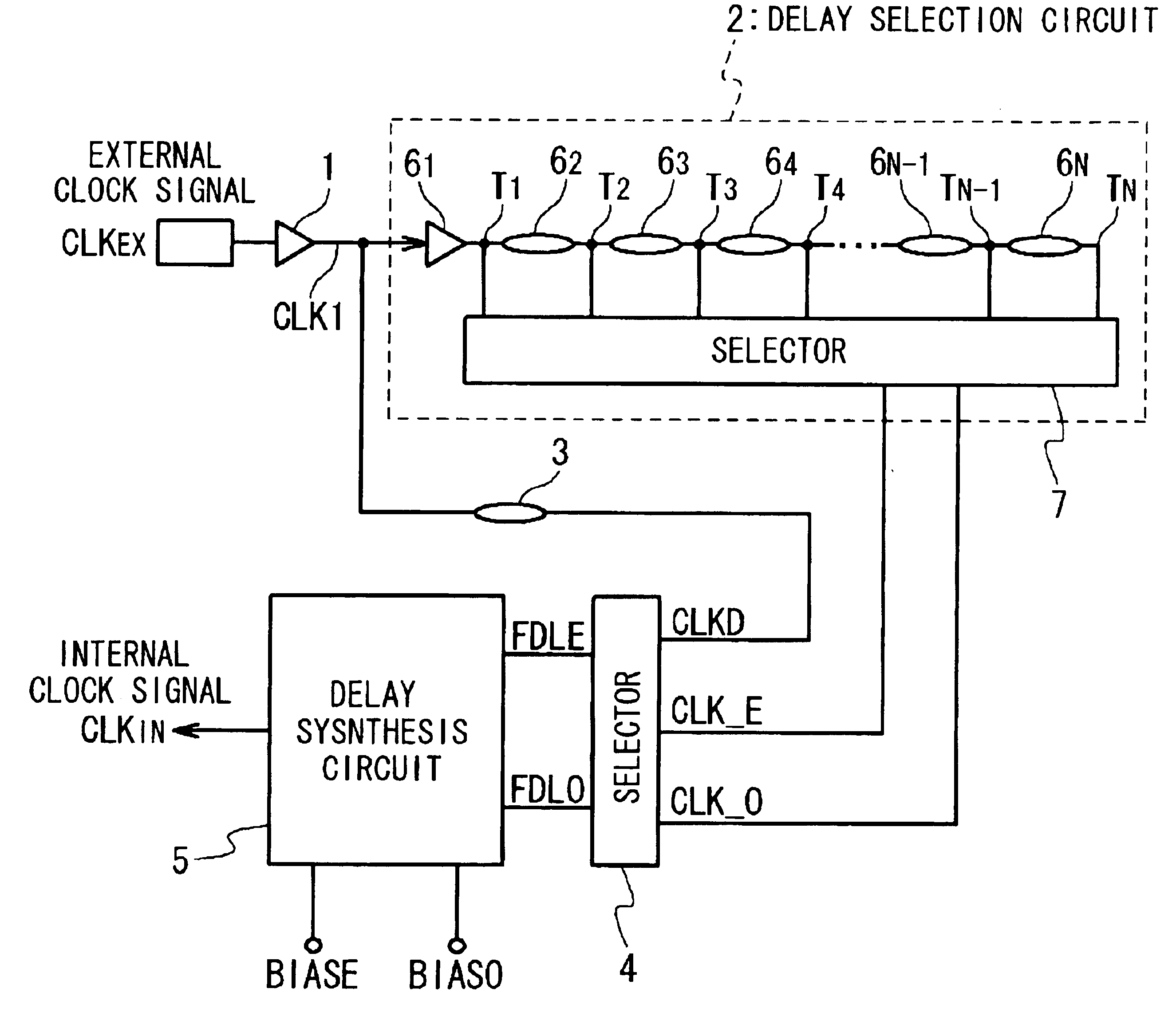
[0046]As is shown in FIG. 1, an embodiment of the present invention is a DLL circuit that delays an external clock signal CLKEX supplied from its outside by a desired delay time to generate an internal clock signal CLKIN. The DLL circuit includes an input buffer 1, a delay selection circuit 2, a delay device 3, a selector 4, and a delay synthesis circuit 5.

[0047]The input buffer 1 reproduces the waveform of the external clock signal CLKEX supplied to its input terminal to generate a clock signal CLK1. The input buffer 1 outputs the clock signal CLK1 to the delay selection circuit 2. The clock signal CLK1 is input to the delay selection circuit 2.

[0048]The delay selection circuit 2 delays the clock signal CLK1 to generate two clock signals CLK_E and CLK_O. The delay time of the delay selection circuit 2 (i.e. the delay time during which the clock signal CLK_E is generated from the clock signal CLK1 and the delay time during which the clock signal CLK_O is generated from the clock sig...


PUM


Abstract

DLL circuit with a small minimum delay time while allowing a wide range of adjustment of the delay time. The DLL circuit according includes a first delay circuit for delaying an input clock signal (CLK1) to output a plurality of delayed clock signals (T1 to TN), a first selector (7) for selecting a first delayed clock signal (CLK_E) and a second delayed clock signal (CLK_O) from among the plurality of delayed clock signals (T1 to TN), for output, a second delay circuit (3) for delaying the input clock signal (CLK1) to generate a slightly delayed clock signal (CLKD), a second selector (4) for selecting two selected clock signals (FDLE, FDLO) from among the slightly delayed clock signal (CLKD), first delayed clock signal (CLK_E), and second delayed clock signal (CLK_O), and a delay synthesis circuit (5) for generating an internal clock signal (CLKIN) from the selected clock signals (FDLE, FDLO), for output.

Description

FIELD OF THE INVENTION[0001]The present invention relates to a DLL (Delay Locked Loop) circuit. More specifically, the invention relates to the DLL circuit used for delaying a clock signal by a desired delay time to generate an internal clock signal used in the inside of a semiconductor device.BACKGROUND OF THE INVENTION[0002]Semiconductor devices sometimes have a DLL circuit for delaying an external clock signal supplied from the outside of the semiconductor devices by a desired delay time to generate an internal clock signal. In a synchronous memory, for example, in order to output data in synchronization with an external clock signal, the internal clock signal is generated from the external clock signal, and the timing of outputting the data is synchronized with the internal clock signal. In view of the delay time of a circuit for outputting the data, the internal clock signal is generated to have a phase so that the timing of outputting the data from the synchronous memory match...

Claims


Application Information

Patent Timeline
Patent Type & Authority Patents(United States)
IPC IPC(8): G06F1/10G11C11/407G11C11/4076H03K5/13H03L7/081
CPCH03L7/0814H03L7/0818
Inventor ISHIKAWA, TORU
Owner LONGITUDE SEMICON S A R L
Why Eureka
Try Eureka