Apparatus and method for converting analog signal to pulse-width-modulated signal

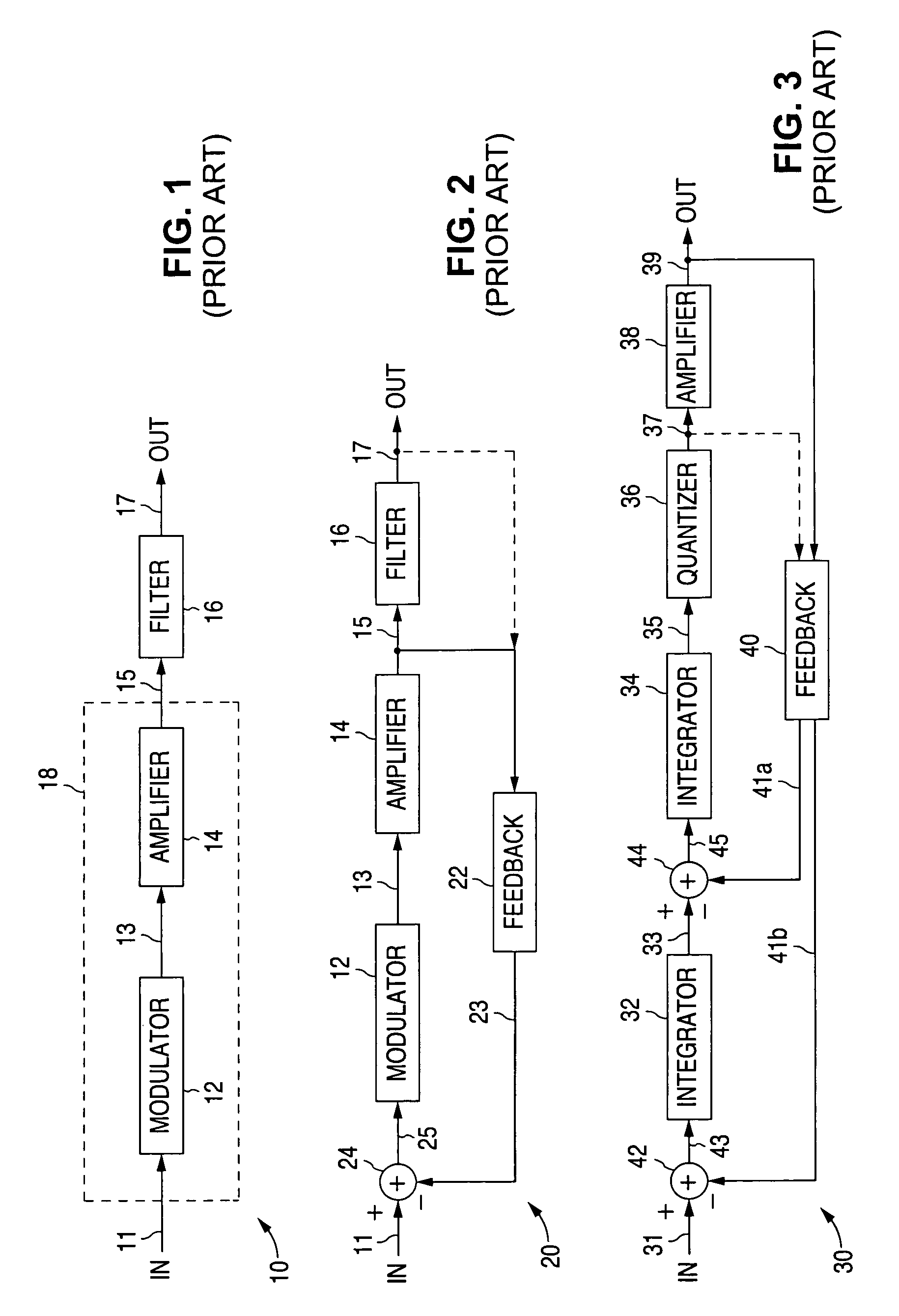
a technology of analog signal and pulse width, applied in pulse technique, code conversion, instruments, etc., can solve the problems of inability to achieve difficulty in creating a system stable and still having high gain and wide bandwidth, and inability to achieve very large in-band gain

Inactive Publication Date: 2005-11-29
NAT SEMICON CORP
View PDF25 Cites 95 Cited by
  • Summary
  • Abstract
  • Description
  • Claims
  • Application Information

AI Technical Summary

Benefits of technology

The patented method involves feeding back an analog waveform that has been divided into smaller parts called pulses. These small parts are then used in another way to create a continuous stream of data. This technology can be useful for various applications such as communication systems.

Problems solved by technology

The technical problem addressed in this patent is the problem of power supply ripple being coupled into the output signal of a high-efficiency amplifier system, and the difficulty in creating a stable system with a high gain and wide bandwidth when using a filter with a natural cut-off frequency. The patent proposes a solution involving noise shaping the output signal spectrum using a feedback network, but current techniques have limitations in terms of bandwidth and signal distortion. The patent aims to provide a noise-shaped, high-efficiency amplifier system with less in-band signal noise and less signal distortion than existing systems.

Method used


Image

  • Apparatus and method for converting analog signal to pulse-width-modulated signal
  • Apparatus and method for converting analog signal to pulse-width-modulated signal
  • Apparatus and method for converting analog signal to pulse-width-modulated signal

Examples


Embodiment Construction

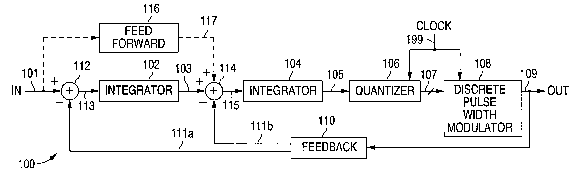
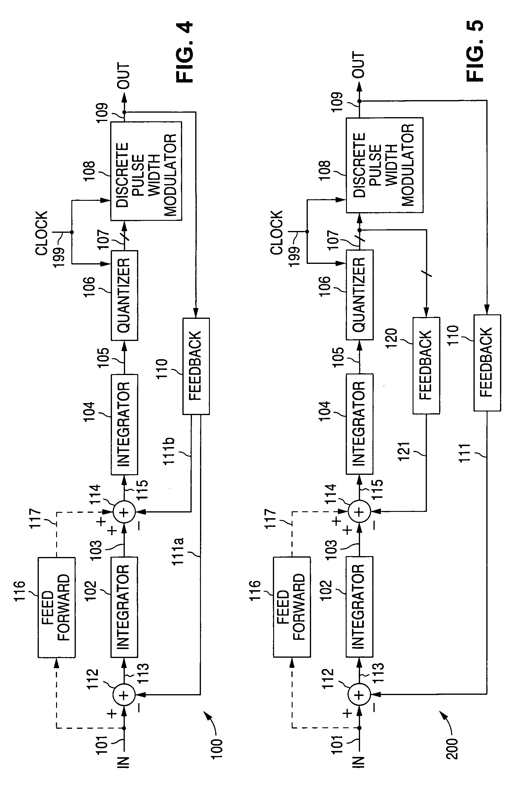
[0027]Referring to FIG. 4, a high-efficiency switching amplifier system 100 using noise shaping techniques in accordance with one embodiment of the present invention includes serially coupled integrators 102, 104, a quantizer 106, a discrete pulse-width modulator 108, a feedback network 110 and signal summers 112, 114, interconnected in a closed loop configuration substantially as shown. The input analog signal 101 is alternately summed with feedback signals 111a, 111b in the signal summers 112, 114 and integrated by the integrators 102, 104, in accordance with well-known delta-sigma techniques. (A second order delta-sigma configuration is shown and discussed herein, but it will be readily understood that higher order delta-sigma techniques can also be used in accordance with the present invention.) The resulting signal 105 is then quantized in a multiple-bit quantizer stage 106, and the multi-bit quantized signal 107 is converted to a discrete time PWM signal 109 by the discrete pu...


PUM


Abstract

A circuit for converting an analog signal to a discrete pulse-width-modulated (PWM) signal uses a delta-sigma amplifier and a discrete PWM stage to produce a discrete PWM output signal having lower in-band signal noise then a PDM system and a lower signal distortion then a continuous PWM system. A multiple bit quantization stage drives the discrete PWM stage.

Description


Claims


Application Information

Patent Timeline
Owner NAT SEMICON CORP
Why Eureka
Try Eureka