Transmit and receive protection circuit

a protection circuit and transmit and receive technology, applied in the field of electronic protection circuits, can solve the problems of loss in the protection circuit, poor matching of discrete diodes, and loss of transmit and receive circuits, etc., and achieve low ac resistance, accurate reproduction, and low loss.

Inactive Publication Date: 2005-12-06
LUCENT TECH INC
View PDF10 Cites 4 Cited by
  • Summary
  • Abstract
  • Description
  • Claims
  • Application Information

AI Technical Summary

Benefits of technology

[0009]The present invention discloses a superior transmit and receive protection circuit for use in a communication system. In the superior transmit and receive protection circuit, the DC currents through an input side and an output side of a four-diode gate are controlled independently. By independently controlling the DC currents through each side of the four-diode gate, more control over the DC currents through the individual diodes of a four-diode gate is achieved. This allows a four-diode gate having low AC resistance to be created in which low power AC signals on an input side of the four-diode gate are accurately reproduced on an output side of the four-diode gate. The invention can be implemented with common resistors, diodes, and capacitors. This arrangement results in an inexpensive, predictable, low loss transmit and receive protection circuit.

Problems solved by technology

However, discrete diodes are notoriously poorly matched, and diodes formed in a common substrate may not be well matched either.
This results in control currents which are unpredictable and vary on the input side 26 and the output side 28, leading to losses in the protection circuit 10.
Unless rigorous matching techniques are applied, the protective circuit may have unacceptable loss.
The matching techniques may be expensive and time consuming, leading to high costs.

Method used


Image

  • Transmit and receive protection circuit
  • Transmit and receive protection circuit
  • Transmit and receive protection circuit

Examples


Embodiment Construction

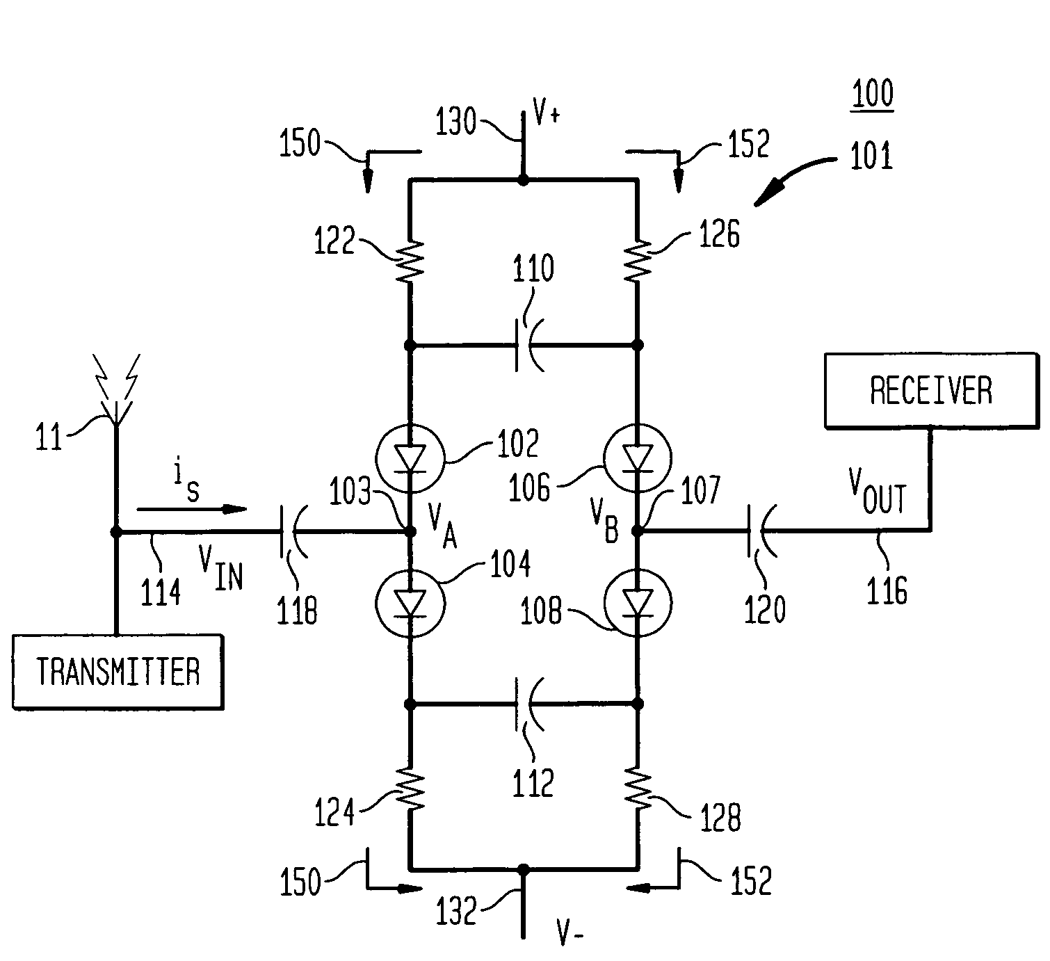
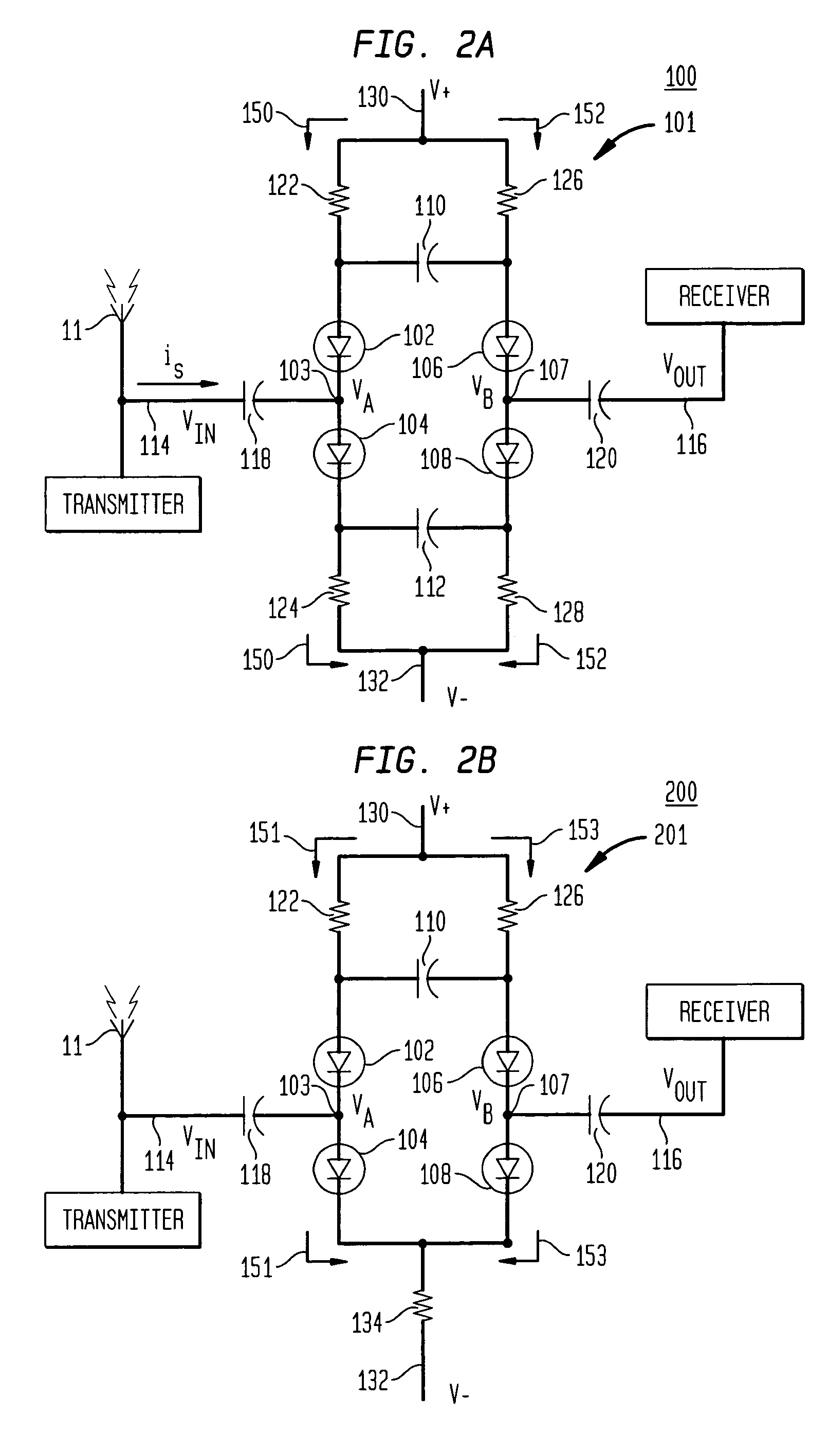
[0016]The present invention discloses a superior transmit and receive protection circuit for use in a communication system. The invention allows the DC current through individual diodes of a four-diode gate to be selectively controlled. By controlling the currents through the individual diodes, the protection circuit can offer improved predictability and loss characteristics without the need for elaborate diode matching. The present invention can be implemented with minimal cost using readily available components.

[0017]FIG. 2A depicts a preferred embodiment of the present invention in an exemplary communication system 100. In the preferred embodiment of the present invention, the protection circuit 101 comprises an input side 150 comprising resistor 122, diode 102, diode 104, and resistor 124 connected in series between a first potential 130 and a second potential 132; and an output side 152 comprising resistor 126, diode 106, diode 108, and resistor 128 connected in series between ...


PUM


Abstract

A transmit and receive protection circuit for use in a communication system is disclosed. The protection circuit uses a four-diode gate in which the currents through an input portion and an output portion of the diode gate are individually controlled by resistors located in their respective portions. This arrangement allows the DC currents through each portion to be independently controlled. By using resistors to independently control the DC currents through each portion of the diode gate, better control over the individual DC currents can be achieved, leading to effective AC resistances which are more predictable. This arrangement results in a predictable low loss protection circuit at a minimal expense.

Description

FIELD OF THE INVENTION[0001]The present invention relates to electronic protection circuits. More particularly, the present invention relates to electronic protection circuits for use in a transceiver between the transmitter and receiver.BACKGROUND OF THE INVENTION[0002]Conventional transmit and receive circuits, such as those found in radio transceivers, contain a protection circuit for isolating a receiver from a transmitter while allowing the receiver to receive signals from an antenna. The protection circuit allows low power AC input signals received at the antenna to pass from the antenna to the receiver, while protecting the receiver from potentially damaging high power AC currents within the transceiver. The high power AC currents may be generated by the transmitter or other components located within the transceiver. The protection circuit is typically coupled between the receiver side and the antenna / transmitter side through AC coupling capacitors to prevent DC currents from...

Claims


Application Information

Patent Timeline
Patent Type & Authority Patents(United States)
IPC IPC(8): H04B1/48H04L23/00
CPCH04B1/48
Inventor MCLELLAN, SCOTT W.
Owner LUCENT TECH INC
Why Eureka
Try Eureka