Semiconductor chip stack structure

a technology of semiconductor chips and stacks, applied in the direction of semiconductor devices, semiconductor/solid-state device details, electrical apparatus, etc., can solve the problems of increasing stack height, electrical interference between them, and substantial stack height increase, so as to achieve the effect of reducing the total height of the semiconductor chip stack

Inactive Publication Date: 2005-12-20
SAMSUNG ELECTRONICS CO LTD
View PDF9 Cites 56 Cited by
  • Summary
  • Abstract
  • Description
  • Claims
  • Application Information

AI Technical Summary

Benefits of technology

[0012]The present invention is directed to forming a semiconductor chip stack structure, with which the total height of semiconductor chip stack can be reduced regardless of the size of a second chip.

Problems solved by technology

The three-dimensional stack of the packaged chips, however, increases the stack height due to individual package thickness.
Such a spacer, unfortunately, causes a substantial increase in the stack height.
Thus, electrical interference between them may occur.
As described above, the conventional chip stack technology has a disadvantage of increasing the total stack height due to the spacer required between the semiconductor chips.

Method used


Image

  • Semiconductor chip stack structure
  • Semiconductor chip stack structure
  • Semiconductor chip stack structure

Examples


Embodiment Construction

[0026]Preferred embodiments of the present invention will be described below with reference to the accompanying drawings. Like reference numerals refer to like elements throughout the drawings.

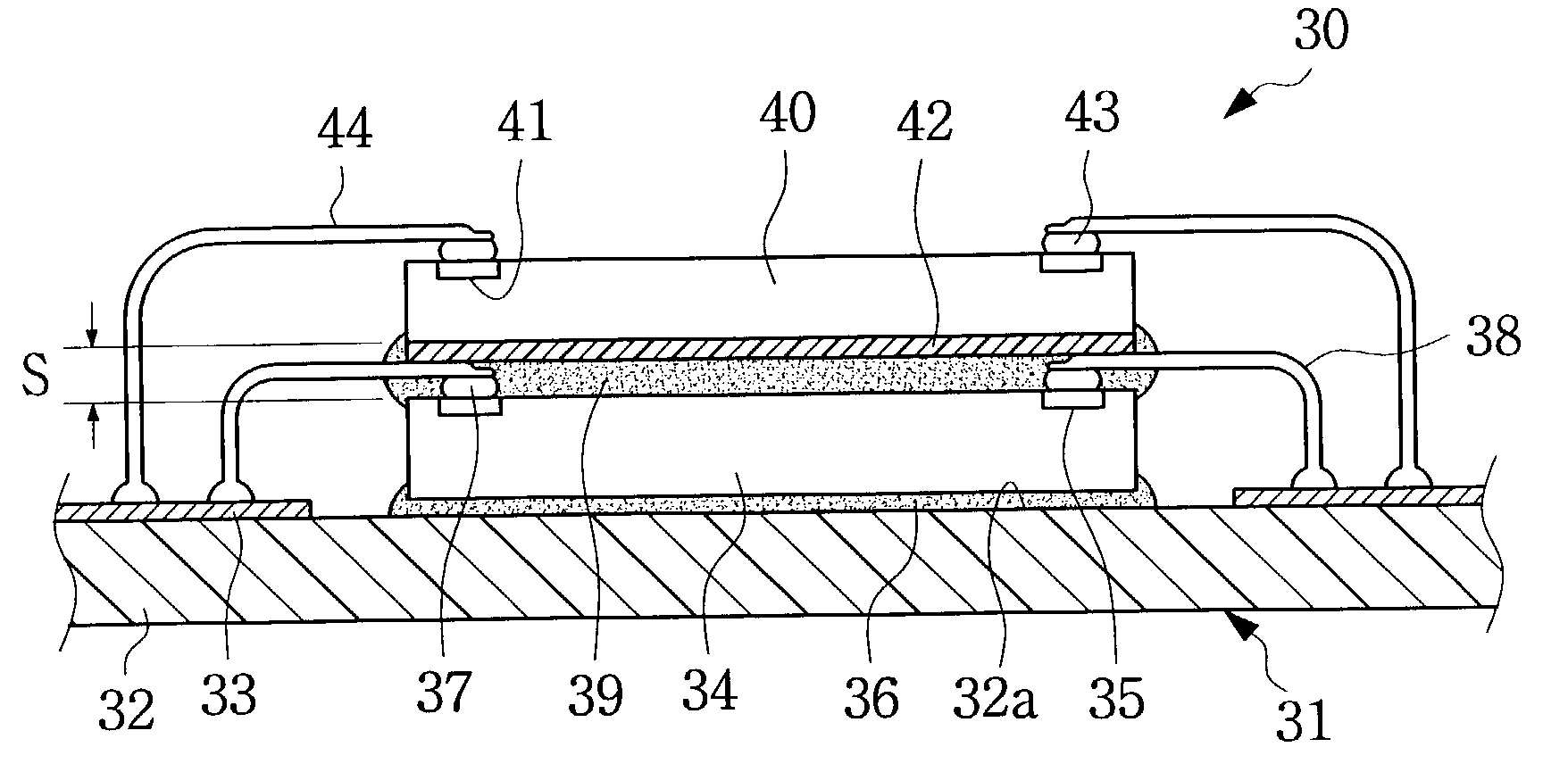
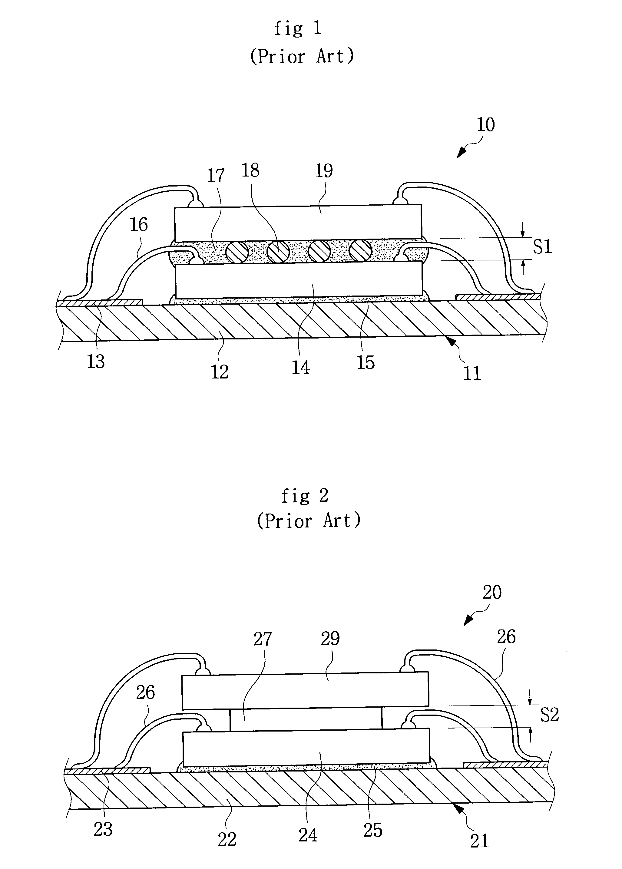
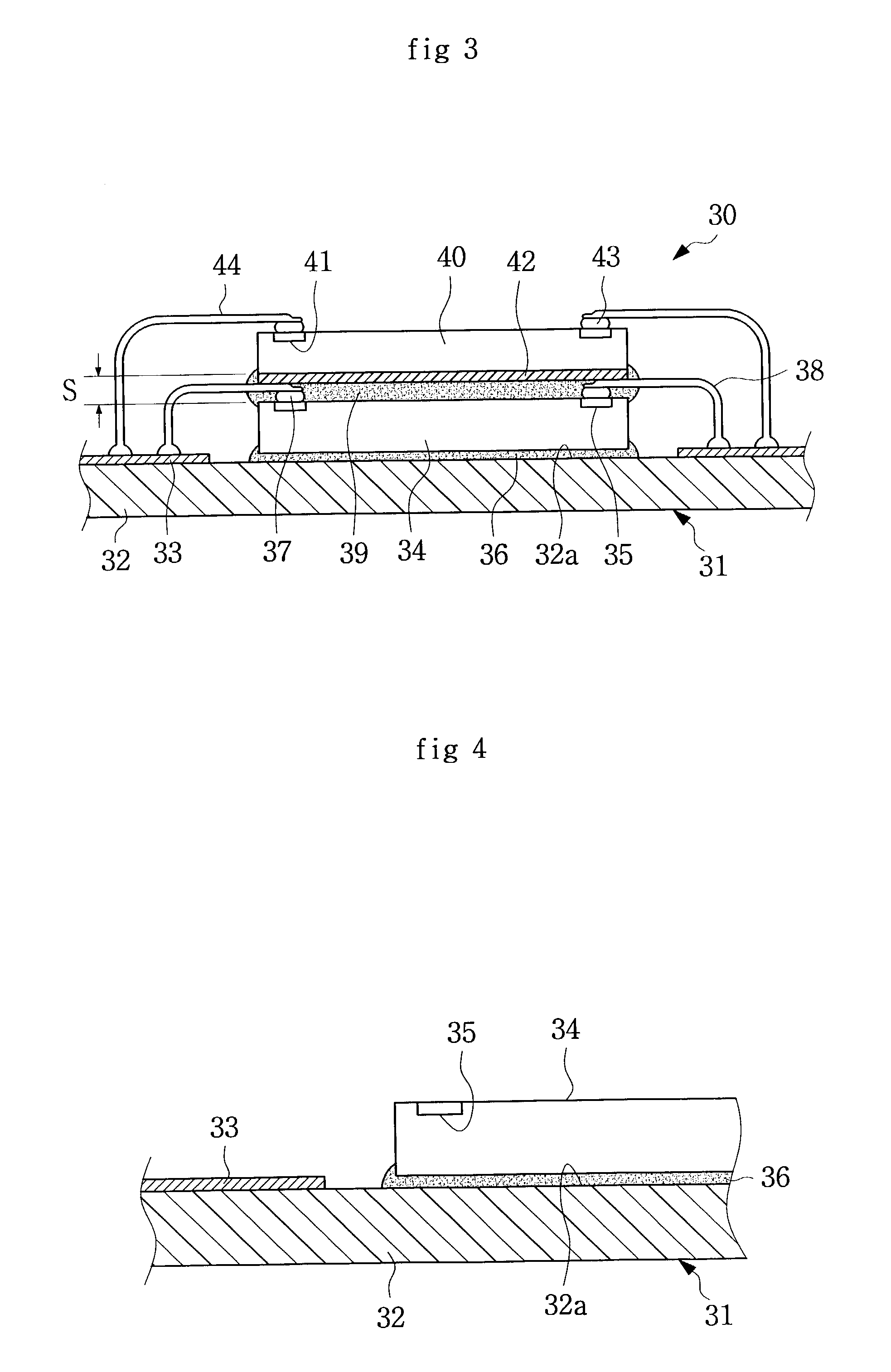
[0027]FIG. 3 is a cross-sectional view of a semiconductor chip stack structure in accordance with one embodiment of the present invention. Referring to FIG. 3, a first semiconductor chip 34 and a second semiconductor chip 40 are sequentially stacked on a substrate 31. To minimize a space S between both chips 34 and 40, an insulating adhesive layer 42 is formed on the bottom surface of the second chip 40 and is in contact with a first bonding wire 38 on the first chip 34.

[0028]The substrate 31 may be a conventional printed circuit board. The substrate 31 includes a substrate body 32 having a die-mounting surface 32a, and wiring patterns 33 surrounding the die-mounting surface 32a on the substrate body 32. Although the preferred embodiment of the present invention employs the printed circuit boa...


PUM


Abstract

Semiconductor chip stack structure and method are provided. A first chip has a first metal bump formed on a first electrode pad. The first chip is attached to and electrically connected to a substrate. The electrical connection is made by a bump reverse bonding method in which one end of a bonding wire is ball-bonded to the substrate and the other end is stitch-bonded to the metal bump. The second chip is stacked on the first chip. The bonding wire is substantially parallel with a top surface of the first chip. Accordingly, the chip stack structure and method minimize a space between the first chip and the second chip, thereby reducing the total height of semiconductor chip stack.

Description

RELATED APPLICATION[0001]This application claims priority from Korean Patent Application No. 2002-15329, filed on Mar. 21, 2002, the contents of which are incorporated herein by reference in their entirety.BACKGROUND OF THE INVENTION[0002]1. Field of the Invention[0003]The present invention relates to a semiconductor packaging technology and, more particularly, to a semiconductor chip stack structure and method for forming the same.[0004]2. Description of the Related Art[0005]To provide improved performance, manufacturers of integrated circuit (IC) chips continually strive to increase packaging density, which has led to the development of, for example, a three-dimensional chip stack technology. In this technology, typically, after the wafer is separated into individual chips, the chips are stacked before or after they are packaged.[0006]The three-dimensional stack of the packaged chips, however, increases the stack height due to individual package thickness. In contrast, the three-d...

Claims


Application Information

Patent Timeline
Patent Type & Authority Patents(United States)
IPC IPC(8): H01L23/12H01L25/065
CPCH01L24/85H01L25/0657H01L24/48H01L24/29H01L2924/07802H01L2224/05599H01L2224/2919H01L2224/2929H01L2224/29339H01L2224/30505H01L2224/48091H01L2224/48095H01L2224/48227H01L2224/48465H01L2224/48471H01L2224/48479H01L2224/73265H01L2224/85051H01L2224/85186H01L2224/85399H01L2224/85986H01L2224/92247H01L2225/0651H01L2225/06513H01L2225/06575H01L2924/01005H01L2924/01006H01L2924/01047H01L2924/01082H01L2924/14H01L2924/00014H01L2924/01033H01L2224/32145H01L2224/32225H01L2224/83139H01L2924/12041H01L2924/0715H01L2924/0665H01L2224/78H01L2224/45099H01L2924/00H01L2924/00012H01L24/73H01L2924/15787H01L2224/4554H01L23/12
Inventor KANG, IN-KUAHN, SANG-HOYANG, SUN-MO
Owner SAMSUNG ELECTRONICS CO LTD
Why Eureka
Try Eureka