Zero insertion force dual beam surface mount contact

a technology of surface mount contact and zero insertion force, which is applied in the manufacture of contact parts, fixed connections, coupling device connections, etc., can solve the problems of contact beams, contact bodies, and inability to form stamping, and achieve the effect of reducing the number of contact beams

Inactive Publication Date: 2005-12-27
TE CONNECTIVITY CORP
View PDF7 Cites 11 Cited by
  • Summary
  • Abstract
  • Description
  • Claims
  • Application Information

AI Technical Summary

Problems solved by technology

One drawback in this configuration is that the contact beams, due to their orientation with respect to the contact body, cannot be formed by stamping in a two-piece die.
Rather, the beams are shaped in free space which makes dimensions and tolerances difficult to control.
The aforementioned developments and advances present ongoing challenges for both simplified connector designs as well as manufacturing methods that reduce product cost while overcoming the drawbacks with current manufacturing processes.

Method used


Image

  • Zero insertion force dual beam surface mount contact
  • Zero insertion force dual beam surface mount contact
  • Zero insertion force dual beam surface mount contact

Examples


Embodiment Construction

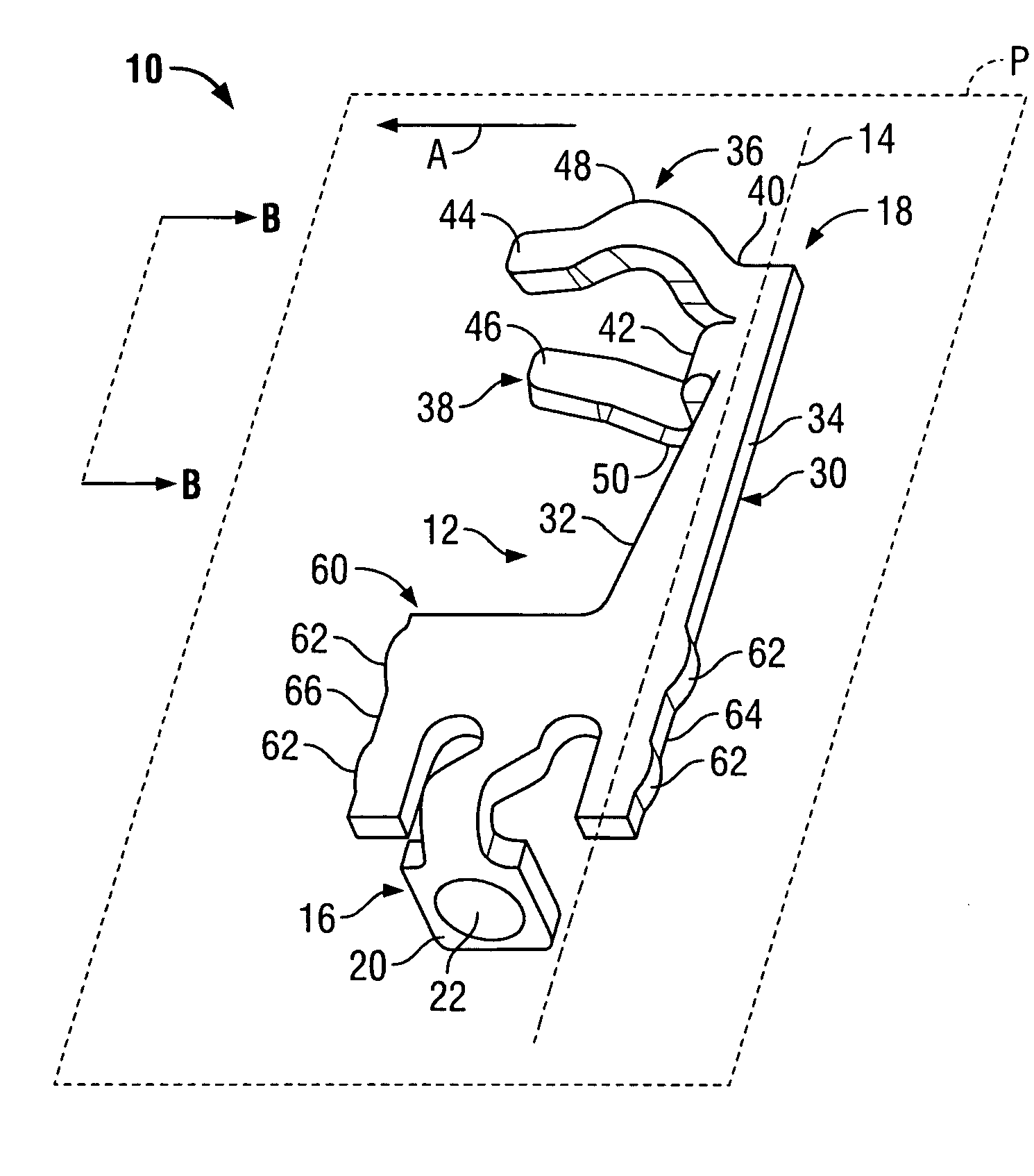
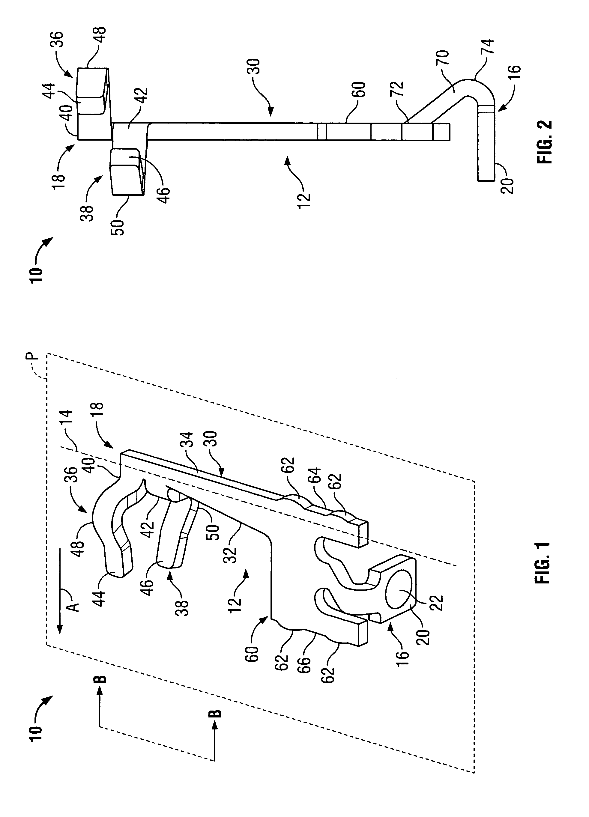
[0022]FIG. 1 illustrates a perspective view of an electrical contact 10 formed in accordance with an exemplary embodiment of the present invention. The contact 10 is a zero insertion force (ZIF) contact adapted for use in an array socket connector such as a micro pin grid array (Micro PGA) connector. It is appreciated, however, that the benefits and advantages of the invention may accrue equally to other types of connectors and sockets across a variety of circuit board connector applications. Therefore, while the invention is described and illustrated in the context of a PGA connector contact 10, the invention is not intended to be limited to such an application, and the description below is therefore provided for purposes of illustration rather than limitation.

[0023]As shown in FIG. 1, the contact 10 includes a contact body 12 that defines contact plane P and a longitudinal contact axis 14. The contact body 12 includes a contact mounting end 16 that is provided for attachment of th...


PUM


Abstract

An electrical contact for a connector includes a contact body that defines a contact plane and a longitudinal contact axis. The contact body includes a contact mounting end for attaching the contact to a circuit board, a mating end to mate with a mating contact, and a backbone section including first and second opposite edges that longitudinally extends between the mating and mounting ends. The mating end includes first and second contact beams laterally extending from the first edge and longitudinally displaced from one another the longitudinal axis.

Description

BACKGROUND OF THE INVENTION[0001]The invention relates generally to surface mounted connectors on circuit boards, and more specifically to a zero insertion force contact for a grid array connector.[0002]With the ongoing trend toward smaller, faster, and higher performance electrical components such as processors used in computers, it has become increasingly important for other components in the processors' electrical paths to also operate at higher speeds. It is also important that the electrical interfaces connecting the various components to a circuit board become faster. Grid array interfaces, along with surface mount technology, have been developed in response to the need for faster and higher density electrical circuits. As is known in the art, surface mountable packaging allows for the connection of an electronic module, or package, to pads on the surface of the circuit board rather than by contacts or pins soldered in plated holes going through the circuit board.[0003]A Pin G...

Claims


Application Information

Patent Timeline
Patent Type & Authority Patents(United States)
IPC IPC(8): H01R4/50H01R12/16H01R12/55H01R13/193H01R13/24H01R13/625H01R43/16
CPCH01R13/193H01R43/16H01R12/716H01R12/707H05K7/1084
Inventor SCHOLZ, JAMES PAUL
Owner TE CONNECTIVITY CORP
Why Eureka
Try Eureka