Amplification type solid-state imaging device having a potential detecting circuit for each unit cell and high-speed readout method thereof

Active Publication Date: 2006-01-03
KK TOSHIBA
View PDF16 Cites 50 Cited by
  • Summary
  • Abstract
  • Description
  • Claims
  • Application Information

AI Technical Summary

Benefits of technology

[0041]FIG. 1 is a circuit diagram for illustrating the conventional solid-state imaging device;
[0042]FIG. 2 is a timing chart showing conventional pulse timings used for driving the solid-state imaging device shown in FIG. 1;
[0043]FIG. 3 is a timing chart showing the correlation between the conventional horizontal readout pulse and clear

Problems solved by technology

In this case, however, there occurs a problem that the S/N ratio is lowered by a variation in the characteristic of the potential detecting circuit provided for each unit cell and studies on this matter are actively continued.
However, since the symmetry of the circuit arrangement and patt

Method used


Image

  • Amplification type solid-state imaging device having a potential detecting circuit for each unit cell and high-speed readout method thereof
  • Amplification type solid-state imaging device having a potential detecting circuit for each unit cell and high-speed readout method thereof
  • Amplification type solid-state imaging device having a potential detecting circuit for each unit cell and high-speed readout method thereof

Examples


first embodiment

[0053][First Embodiment]

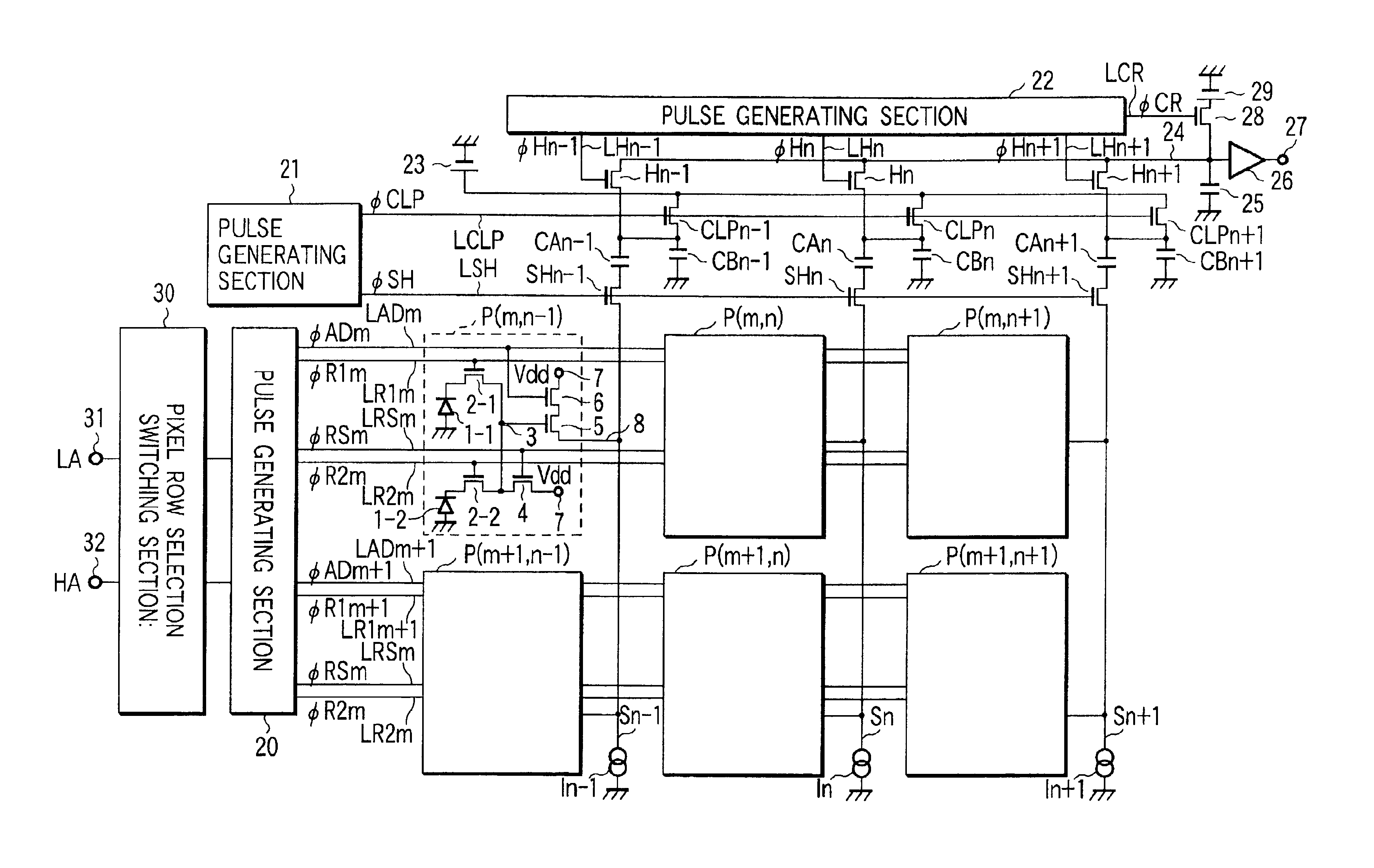
[0054]FIG. 6 is a circuit diagram showing the construction of a solid-state imaging device according to one embodiment of this invention. Like the case of FIG. 1, in FIG. 6, a solid-state imaging device having two photodiodes arranged in each unit cell is taken as an example.

[0055]Unit cells are arranged in a two-dimensional fashion in an imaging area on a semiconductor substrate. More precisely, the unit cells are arranged in i rows and j columns, where i and j are integers. Of these unit cells, six representive ones are illustrated in FIG. 6. The six unit cells P are arranged in two adjacent rows m and m+1 and three adjacent columns n−1, n and n+1; they are located at intersections (m, n−1), (m, n), (m, n+1), (m+1, n−1), (m+1, n) and (m+1, n+1).

[0056]An address pulse line LADi, first and second readout pulse lines LR1i, LR2i and reset pulse line LRSi are arranged in the horizontal direction for each pixel row of the unit cells P(i,j). The unit cells P(i,j) ...

second embodiment

[0078][Second Embodiment]

[0079]FIG. 8 is a circuit diagram for illustrating a solid-state imaging device according to a second embodiment of this invention. The circuit is similar to that of FIG. 6 except that a pixel column selection circuit 40 and pixel column selection information processing circuit (decoder) 41 are provided instead of the pixel row selection switching circuit 30 and input terminals 31, 32 in the circuit of FIG. 6. A signal SCA for selecting a pixel column is supplied to and decoded by the pixel column selection information processing circuit 41 and the decoded signal SCA is supplied to the pixel column selection circuit 40. The pixel column selection circuit 40 controls the pulse generating section 22 and causes the pulse generating section 22 to output a horizontal readout pulse at different timings according to the high-resolution mode and high-speed driving mode.

[0080]Since the other basic construction is the same as that of the circuit of FIG. 6, like portio...

third embodiment

[0086][Third Embodiment]

[0087]FIG. 10 is a circuit diagram for illustrating a solid-state imaging device according to a third embodiment of this invention. The circuit is basically similar to that of FIG. 8 except that the control operation for controlling the pulse generating section 22 by use of a pixel column selection circuit 40′ and pixel column selection information processing circuit (decoder) 41′ is different, and as shown in the timing chart of FIG. 11, horizontal readout transistors arranged for every three unit cells are turned ON at the same timing. That is, signal charges are simultaneously read out from every third columns of unit cells by simultaneously setting the horizontal readout pulses φH1 and φH4, φH2 and φH5, φH3 and φH6, to the high level and the average value thereof is output.

[0088]Therefore, the average value is output at the pulse repetition rate of the horizontal readout pulse. The readout method described in the third embodiment is preferable for a const...


PUM


Abstract

A solid-state imaging device comprising an imaging area having unit cells, a vertical driving circuit, signal processing circuits, a horizontal driving circuit, and an output circuit. Each of the unit cells including first and second photoelectric conversion/storage sections, first and second charge readout circuits, a potential detecting circuit, a reset circuit, and an address circuit. The solid-state imaging device has a first operation mode in which the first and second charge readout circuits are driven at substantially the same timing by the vertical driving circuit, the charges stored in the first and second photoelectric conversion/storage sections are transferred to and added together in the charge detecting section, and the potential detecting circuit detects the added charges, generates and transmits a potential corresponding to an amount of detected charges to the vertical signal line, and outputs the potential from the output circuit via the signal processing circuits.

Description

CROSS-REFERENCE TO RELATED APPLICATIONS[0001]This application is based upon and claims the benefit of priority from the prior Japanese Patent Application No. 2000-090061, filed Mar. 29, 2000, the entire contents of which are incorporated herein by reference.BACKGROUND OF THE INVENTION[0002]This invention relates to a so-called amplification type solid-state imaging device having a potential detecting circuit for each unit cell and a high-speed readout method thereof and more particularly to a solid-state imaging device which is operated at high speed while suppressing a lowering in the signal-noise ratio (S / N ratio).[0003]Recently, solid-state imaging devices which are called amplification type solid-state imaging devices each having a potential detecting circuit for each unit cell are actively developed. In comparison with a CCD type solid-state imaging device conventionally used, since the charge transfer operation is effected only in an area around the photodiodes in this type of...

Claims


Application Information

Patent Timeline
IPC IPC(8): H04N3/14H04N5/335H04N5/341H04N5/347H04N5/369H04N5/374H04N5/3745
CPCH04N3/1562H04N25/46H04N25/778H04N25/42H04N25/60
Inventor GOTO, HIROSHIGE
Owner KK TOSHIBA
Why Eureka
Try Eureka