Plasma display panel and method of driving the same

a technology of display panel and display panel, which is applied in the direction of static indicating device, address electrode, instrument, etc., can solve the problems of difficult implementation, complicated driving scheme of display brightness and luminescent efficiency using volume discharge effect, etc., and achieve the effect of broadening the operational range of sustain voltage and preventing erasure of written data

Inactive Publication Date: 2006-01-10
AU OPTRONICS CORP
View PDF3 Cites 4 Cited by
  • Summary
  • Abstract
  • Description
  • Claims
  • Application Information

AI Technical Summary

Benefits of technology

[0012]The present invention achieves the above-indicated objects by providing a method of driving a plasma display panel having a sustain electrode and scan electrodes located on the front substrate in parallel and having address electrodes located on the rear substrate. During the sustain periods, a first sustain pulse is transmitted to the sustain electrode and the address electrodes forming positive voltage differences between the sustain electrode and the scan electrodes and between the address electrodes and the scan electrodes. In addition, during the sustain period, a second sustain pulse is alternately transmitted to the scan electrodes for forming negative voltage difference between the sustain electrode and the scan electrodes and between the address electrodes and the scan electrodes. It is noted that the first sustain pulse and the second sustain pulse are square-wave and out of phase. In addition, the maximal voltage of the first sustain pulse and the second sustain pulse is lower than the firing voltages between the sustain electrode and the scan electrodes and between the address electrodes and the scan electrodes, preventing erasure of the written data. Thus, the firing voltages between these electrodes must be high enough to broaden the operational range of the sustain voltage of the sustain pulses. There are four novel structures of the plasma display panel to raise the firing voltage in the present invention.

Problems solved by technology

Conventional proposals for improving the display brightness and luminescent efficiency using the volume discharge effect usually adopt complicated driving schemes, not easily implemented.

Method used


Image

  • Plasma display panel and method of driving the same
  • Plasma display panel and method of driving the same
  • Plasma display panel and method of driving the same

Examples


first embodiment

[0026]The present invention employs the volume discharge effect to improve the display brightness and luminescent efficiency of the PDP during the sustain periods. More specifically, during the sustain periods, as well as the voltage applied between the sustain electrode X and the scan electrode Yi, an auxiliary voltage is additionally applied between the address electrode Ai and the scan electrode Yi. In the present invention, the same driving signal is sent to the sustain electrode X as well as the address electrode Ai at the same time to achieve the desired volume discharge effect.

[0027]FIGS. 6A and 6B are schematic diagrams illustrating the volume discharge effect in accordance with the present invention. In FIG. 6A, the sustain pulses with an amplitude of voltage Vs are sent to the sustain electrode X and the address electrode Ai, respectively, where the voltage on the scan electrode Yi is 0V. Therefore, the wall charges (i. e. the positive ions) accumulated in the display cell...

second embodiment

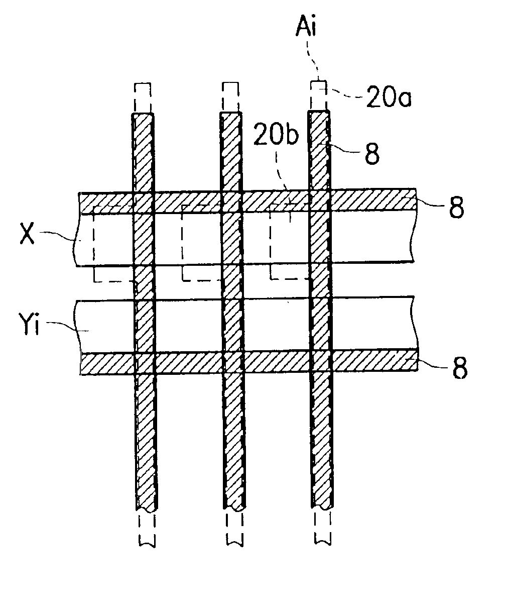
[0032]The first embodiment employs the scheme of redesigning address electrodes to raise the firing voltage between the address electrode Ai and the scan electrode Yi and to broaden the operational range of the sustain voltage. The present embodiment adopts a different design to achieve the same object.

[0033]FIG. 9 is a top view of the PDP in accordance with the second embodiment of the present invention. As shown in FIG. 9, the sustain electrode X and the scan electrodes Yi remain unchanged and the address electrodes Ai are redesigned. In the present embodiment, the address electrode Ai is still located on the rear substrate but divided into two parts with different widths. Part 30a is narrower. Part 30b is wider and is located just under the sustain electrode X on the front substrate. Conventional address electrodes have a uniform width, about 80˜100 μm. In the present embodiment, the width of part 30a of the address electrode is about 50 μm and the width of part 30b is about 150 ...

third embodiment

[0034]The first and second embodiments employ the scheme of redesigning the address electrodes to raise the firing voltage between the address electrodes Ai and the scan electrodes Yi. In the present embodiment, the distances between the sustain electrode X and the address electrode Ai and between the scan electrode Yi and the address electrode Ai are altered to adjust the firing voltage.

[0035]FIG. 10 is a cross-section of the display cell of the PDP in accordance with the third embodiment of the present invention. As shown in FIG. 10, the address electrode Ai remains unchanged but the distances between the sustain electrode X′ and the address electrode Ai and between the scan electrode Yi′ and the address electrode Ai are different. In other words, the sustain electrode X′ and the scan electrode Yi′ are not located on the same plane. In the present embodiment, the vertical distance from the sustain electrode X′ to the substrate 1 is longer than the vertical distance from the scan e...


PUM


Abstract

A method of driving a plasma display panel to improve display brightness and luminescent efficiency. In the sustain periods, the same driving signal is sent to the sustain electrode X as well as the address electrode Ai at the same time to achieve the desired volume discharge effect. In addition, the structure of PDPs is modified to raise firing voltages between these electrodes, preventing erasure of the data written in the address periods.

Description

BACKGROUND OF THE INVENTION[0001]1. Field of the Invention[0002]The present invention relates to a plasma display panel (hereafter called PDP) technology, more specifically, to a plasma display panel and a method of driving the plasma display panel to improve the brightness thereof using volume discharge effect.[0003]2. Description of the Prior Art[0004]The PDP is a display device employing charges accumulated by electrode discharge. Due to a variety of advantages, such as large scale, high capacity and full-color capability, the PDP has become one of the most popular flat panels in various applications.[0005]FIG. 1 is a cross-section of the display cell of a conventional triple-electrode PDP. As shown in FIG. 1, the PDP has two glass substrates 1 and 7. Inert gas, such as Ne and Xe, is filled in a cavity between the glass substrates 1 and 7. Two types of electrodes, including sustain electrode X and scan electrodes Yi, are formed on the glass substrate 1 and parallel to each other....

Claims


Application Information

Patent Timeline
Patent Type & Authority Patents(United States)
IPC IPC(8): H01J17/49G09G3/294H01J11/12H01J11/26H01J11/28
CPCG09G3/2942H01J11/28H01J11/26H01J11/12
Inventor CHIEN, YU-TINGLO, SHIN-TAI
Owner AU OPTRONICS CORP
Why Eureka
Try Eureka