Delay locked loops having delay time compensation and methods for compensating for delay time of the delay locked loops

Inactive Publication Date: 2006-01-17
SAMSUNG ELECTRONICS CO LTD
View PDF7 Cites 7 Cited by
  • Summary
  • Abstract
  • Description
  • Claims
  • Application Information

AI Technical Summary

Benefits of technology

[0021]In additional embodiments of the present invention, the pull-down circuit controls the delay time by

Problems solved by technology

However, it is very difficult to do this in practice.
Moreover, such large loads, typically, cannot be implemented inside the memory chip.
However, since the second external voltage VDDQ may include a large amount of noise, it may have a detrimental influence on the operation of the DLL 50.
Therefore, it may be ineffective to use the second external voltage VDDQ in the compensation delay circuit 55.

Method used


Image

  • Delay locked loops having delay time compensation and methods for compensating for delay time of the delay locked loops
  • Delay locked loops having delay time compensation and methods for compensating for delay time of the delay locked loops
  • Delay locked loops having delay time compensation and methods for compensating for delay time of the delay locked loops

Examples


Embodiment Construction

[0036]The present invention will now be described more fully with reference to the accompanying drawings, in which embodiments of the invention are shown. This invention may, however, be embodied in many different forms and should not be construed as being limited to the embodiments set forth herein. Rather, these embodiments are provided so that this disclosure will be thorough and complete, and will fully convey the concept of the invention to those skilled in the art. Unless indicated otherwise, like numbers refer to like elements.

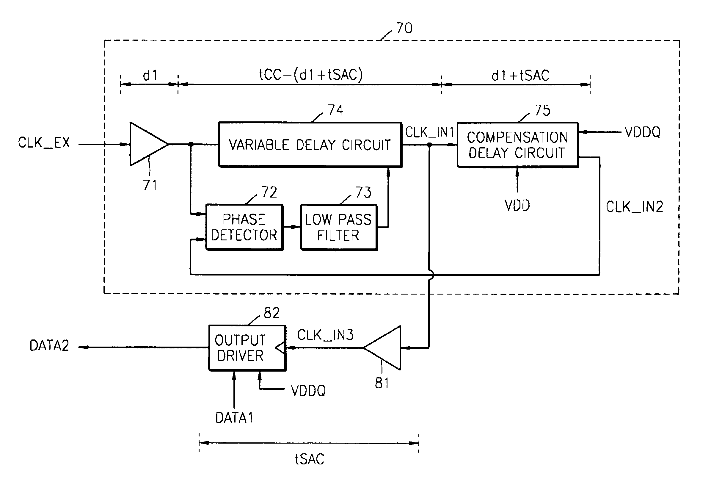
[0037]FIG. 5 is a block diagram of a delay locked loop (DLL) and an output driver of a semiconductor memory device having a compensation delay circuit according to embodiments of the present invention. The DLL and output driver of FIG. 5 may replace the DLL 16 and output driver 17 in a memory device of FIG. 1 to provide memory devices according to embodiments of the present invention. As shown in FIG. 5, a DLL 70 according to embodiments of the present ...


PUM


Abstract

A delay locked loop (DLL) is provided that includes a phase detector configured to detect a phase error between an internal clock signal and the external clock signal and output a phase error signal. A low pass filter is configured to output a predetermined control signal in response to the phase error signal. A variable delay circuit is configured to change a delay time in response to the predetermined control signal, delay the phase of the external clock signal with respect to the changed delay time, lock the delayed external clock signal and output the internal clock signal. A compensation delay circuit is configured to receive a control voltage based on a delay time introduced by a data output circuit and delay a phase of the internal clock signal for a first delay time based on the control voltage and output the delayed internal clock signal to the phase detector. Methods of compensating a delay for a DLL are also provided.

Description

CLAIM OF PRIORITY[0001]This application claims the priority from Korean Patent Application No. 2002-87240, filed on 30 Dec. 2002, in the Korean Intellectual Property Office, the disclosure of which is hereby incorporated by reference in its entirety as if fully set forth herein.FIELD OF THE INVENTION[0002]The present invention relates to a delay locked loops (DLL), and more particularly, to DLLs suitable for use in a memory device.BACKGROUND OF THE INVENTION[0003]In general, voltages supplied to a semiconductor memory device from outside a memory chip include a first external voltage VDD and a second external voltage VDDQ. FIG. 1 is a schematic block diagram of a conventional semiconductor memory device. As shown in FIG. 1, a semiconductor memory device 10 includes power pins 11 and 12, an internal voltage generator 13, a memory cell array 14, a peripheral circuit 15, and an output driver 17. The peripheral circuit 15 includes a delay locked loop (DLL) 16. The first external voltage...

Claims


Application Information

Patent Timeline
IPC IPC(8): H03L7/06G11C8/00G11C7/10H03L7/081
CPCG11C7/1051H03L7/0812G11C7/222G11C7/1066H03L7/0816G11C8/00
Inventor CHUNG, DAE-HYUNSHIN, SANG-WOONGLEE, WOO-JIN
Owner SAMSUNG ELECTRONICS CO LTD
Why Eureka
Try Eureka