Pressure sensor

a pressure sensor and sensor technology, applied in the field of pressure sensors, can solve the problems of difficult to accurately detect pressure in a high temperature environment, greatly deteriorated etc., and achieve the effect of improving the strength of semiconductor substrates and simple pressure sensors

Active Publication Date: 2006-02-14
DENSO CORP
View PDF6 Cites 11 Cited by
  • Summary
  • Abstract
  • Description
  • Claims
  • Application Information

AI Technical Summary

Benefits of technology

[0006]In view of the above-described problems, it is an object of the present invention to provide a pressure sensor, which improves its sensitivity while accurately detecting a pressure of a subject device.
[0009]In the pressure sensor, a bending thickness portion for detecting a pressure is constructed with the thickness part of the diaphragm of the metal stem and the thickness part of the insulation layer. Therefore, a sensitivity of the pressure sensor can be improved and a pressure in a subject device can be accurately detected by using the strain gauges formed on the first semiconductor. For example, the pressure sensor can detect a fuel pressure or a brake pressure.
[0013]As an example, the recess portion is defined by the insulation layer and the second semiconductor layer to have a trapezoid sectional shape enlarged from the insulation layer to a surface of the second semiconductor layer. In this case, the diaphragm has a protrusion portion corresponding to the shape of the recess portion, and the insulation layer of the semiconductor substrate is attached to the surface of the protrusion portion of the diaphragm in the recess portion. Therefore, the structure of the pressure sensor can be made simple.
[0014]Furthermore, the metal stem can be provided with a wall surface extending from the diaphragm outwardly and facing the surface of the second semiconductor layer, and the surface of the second semiconductor layer is attached to the wall surface of the metal stem, outside the recess portion. Therefore, even when the recess portion is provided in the semiconductor substrate, the strength of the semiconductor substrate can be effectively improved.

Problems solved by technology

However, when the semiconductor substrate is made thinner, the strength of the semiconductor substrate is greatly deteriorated.
In this case, a leak current may be generated on the PN junction portion at a high temperature, and it is difficult to accurately detect the pressure at a high temperature environment.

Method used


Image

  • Pressure sensor
  • Pressure sensor
  • Pressure sensor

Examples


first embodiment

(First embodiment)

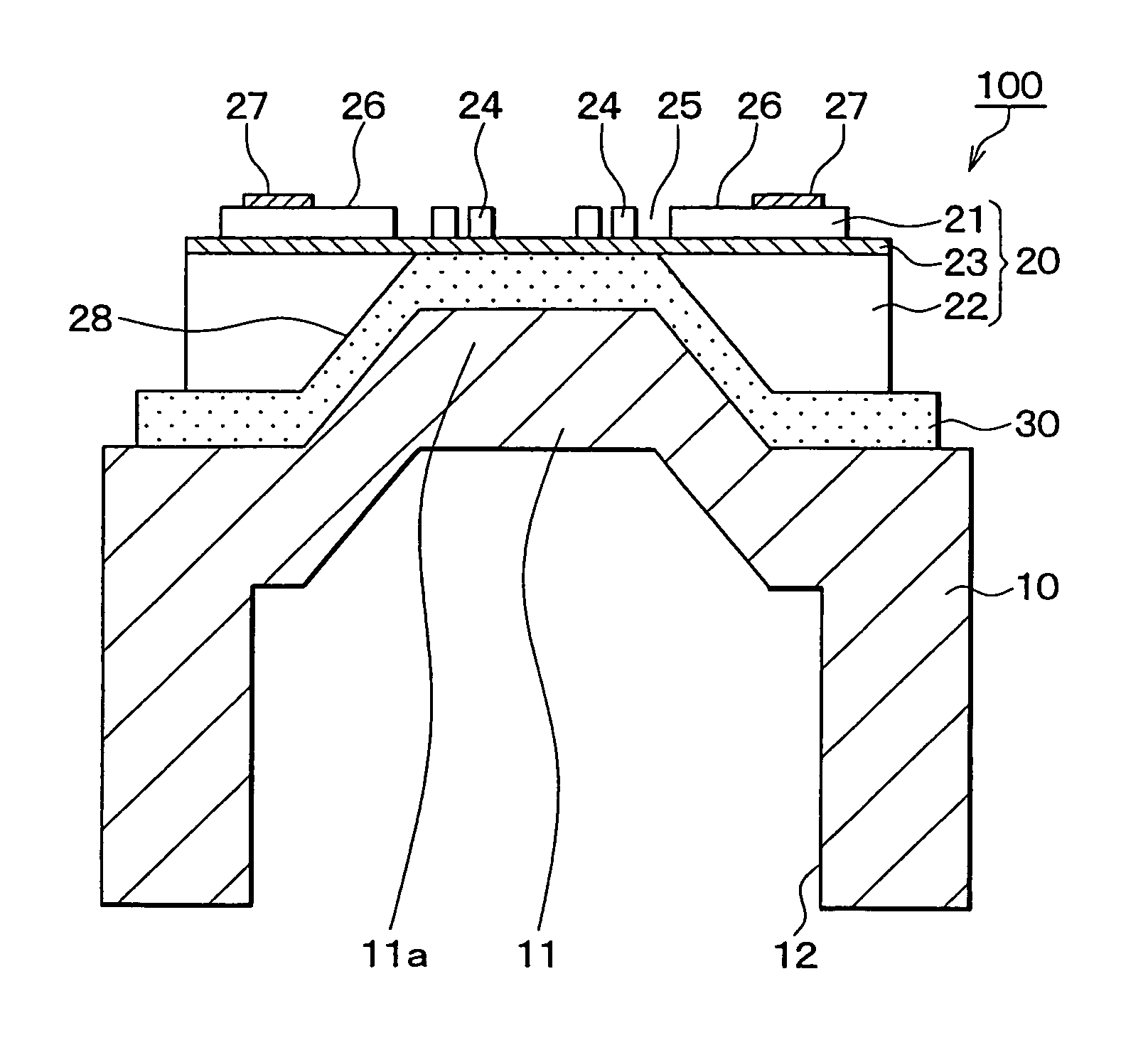
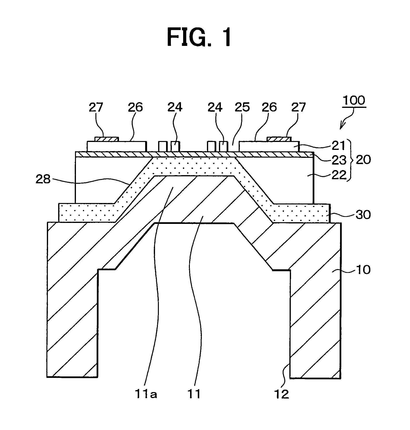
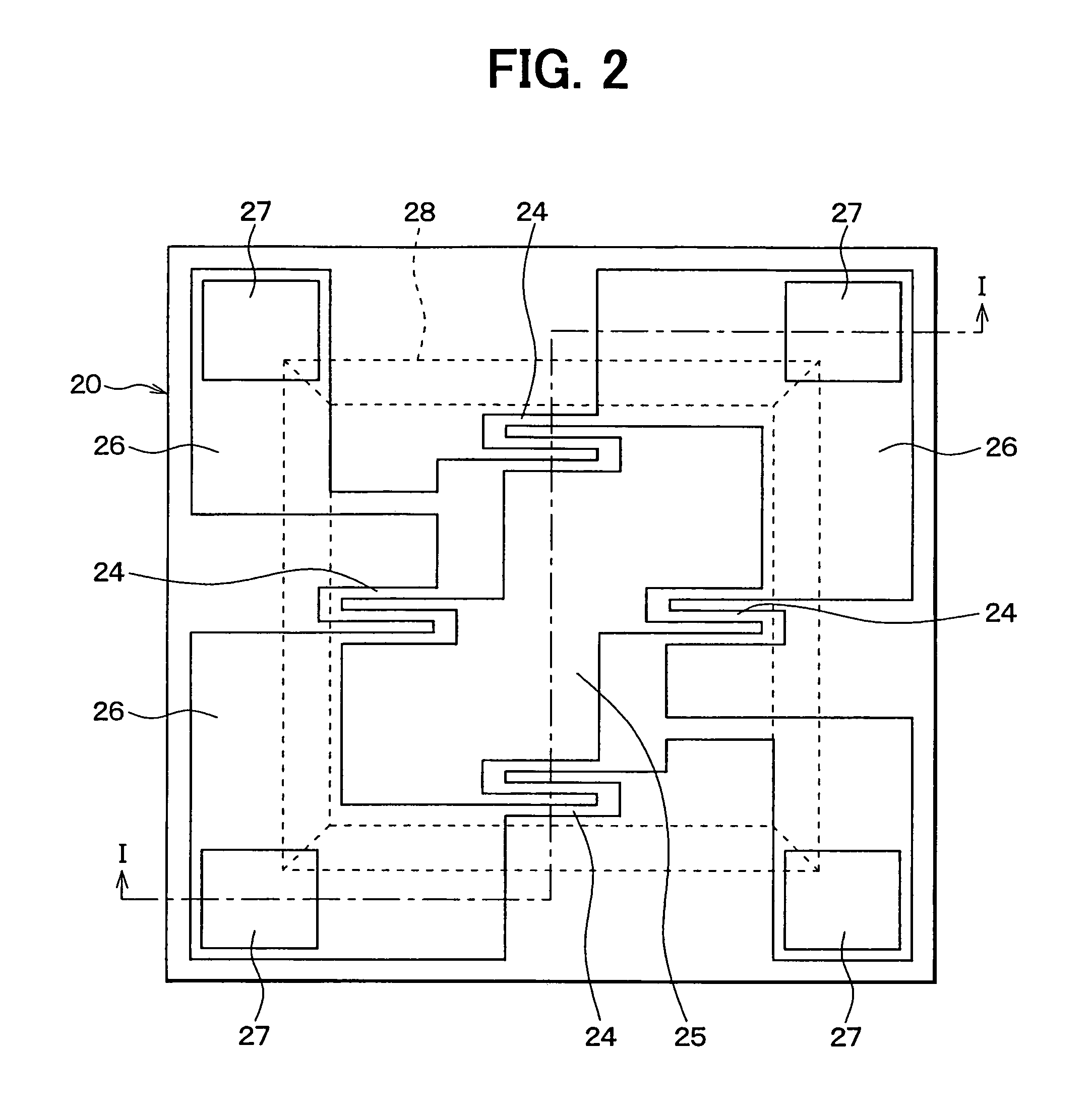
[0020]FIG. 1 shows a pressure sensor 100 and is a sectional view corresponding to a section taken along I—I in FIG. 2. As an example, the pressure sensor 100 can be attached to a subject device, for example, a fuel pipe in a vehicle injection system (e.g., common rail). In this case, the pressure sensor 100 detects the pressure of a liquid fuel or a gas-liquid mixing fuel in the fuel pipe, as a pressure medium.

[0021]The pressure sensor 100 includes a metal stem 10 having a diaphragm 11 for a pressure detection, a semiconductor substrate 20 attached to a surface of the diaphragm 11 in the metal stem 10, and strain gauges 24 for converting a bending (deformation) of the diaphragm 11 to an electrical signal.

[0022]The metal stem 10 is made of a Fe—Ni—Co alloy having a small coefficient of thermal expansion, for example. The metal stem 10 is formed into a hollow cylinder having a closed end portion as shown in FIG. 1. The metal stem 10 has the diaphragm 11 formed as a t...

second embodiment

(Second Embodiment)

[0055]The second embodiment of the present invention will be now described with reference to FIG. 4. In the second embodiment, as shown in FIG. 4, an outer diameter of the diaphragm 11 in the metal stem 10 is made smaller than a diameter of the bottom portion of the recess portion 28.

[0056]As an example, the whole outer diameter of the metal stem 10 can be made smaller than the diameter of the bottom portion (the insulation layer 23) of the recess portion 28 of the semiconductor substrate 20 as shown in FIG. 4. In this case, all the diaphragm 11 is inserted into the recess portion 28, and is readily attached to the insulation layer 23.

[0057]According to the second embodiment, the surface of the diaphragm 11 can be readily attached to the semiconductor substrate 20, and the metal stem 10 can be easily formed because the metal stem 10 has a simple shape.

(Other Embodiments)

[0058]Although the present invention has been described in connection with some preferred embod...


PUM

PropertyMeasurementUnit
thicknessaaaaaaaaaa
thicknessaaaaaaaaaa
pressureaaaaaaaaaa

Abstract

A pressure sensor includes a metal stem having a diaphragm, and a semiconductor substrate in which an insulation layer is inserted between first and second semiconductor layers. A plurality of strain gauges are formed on a predetermined area of the first semiconductor layer of the semiconductor substrate, for converting a bending of the diaphragm to an electrical signal. In the pressure sensor, the strain gauges have pattern shapes insulated and separated from each other by trenches extending from a surface of the first semiconductor layer to the insulation layer. Furthermore, the second semiconductor layer has a recess portion, which is recessed from a surface of the second semiconductor layer to the insulation layer and is provided at a position corresponding to the predetermined area. The diaphragm is inserted into the recess portion, and the insulation layer is attached to a surface of the diaphragm in the recess portion.

Description

CROSS REFERENCE TO RELATED APPLICATION[0001]This application is based on Japanese Patent Application No. 2004-191243 filed on Jun. 29, 2004, the contents of which are incorporated herein by reference in its entirety.FIELD OF THE INVENTION[0002]The present invention relates to a pressure sensor in which a semiconductor substrate having strain gauges is fixed to a surface of a diaphragm of a metal stem. The pressure sensor detects a pressure by converting a bending of the diaphragm to an electrical signal through the strain gauges. The pressure sensor may be suitably used for detecting a pressure in a subject device of a vehicle, for example.BACKGROUND OF THE INVENTION[0003]A pressure sensor includes a metal stem having a diaphragm for a pressure detection, a semiconductor substrate attached to a surface of the diaphragm, and strain gauges for converting a bending of the diaphragm formed on the semiconductor substrate to an electrical signal (for example, JP-B2-7-11461 which correspon...

Claims


Application Information

Patent Timeline
Patent Type & Authority Patents(United States)
IPC IPC(8): G01L9/04G01L9/00
CPCG01L9/0055
Inventor TOYODA, INAO
Owner DENSO CORP
Why Eureka
Try Eureka