Image processing device for layered graphics

a processing device and layer technology, applied in the field of layered graphics, can solve the problems of inability to exchange one layer with the other with a simple command, and the conventional layered graphics device architecture lacks flexibility in reordering the layers in a picture, so as to achieve a simple and easy way to change the order

Inactive Publication Date: 2006-02-14
INTELLECTUAL VENTURES I LLC
View PDF9 Cites 2 Cited by
  • Summary
  • Abstract
  • Description
  • Claims
  • Application Information

AI Technical Summary

Benefits of technology

[0019]In view of the foregoing, it is an object of the present invention to provide an image processing device, as well as a semiconductor chip therefor, which offers a simple and easy way to change the order of layers in a combined picture.

Problems solved by technology

The architecture described above, however, is unable to exchange one layer with another with a simple command, since it requires a memory-to-memory transfer of image data or reconfiguration of address parameters in the memory read units 11a to 11d.
That is, the conventional layered graphics device architecture lacks flexibility in reordering the layers in a picture.

Method used


Image

  • Image processing device for layered graphics
  • Image processing device for layered graphics
  • Image processing device for layered graphics

Examples


Embodiment Construction

[0037]Preferred embodiments of the present invention will be described below with reference to the accompanying drawings, wherein like reference numerals refer to like elements throughout.

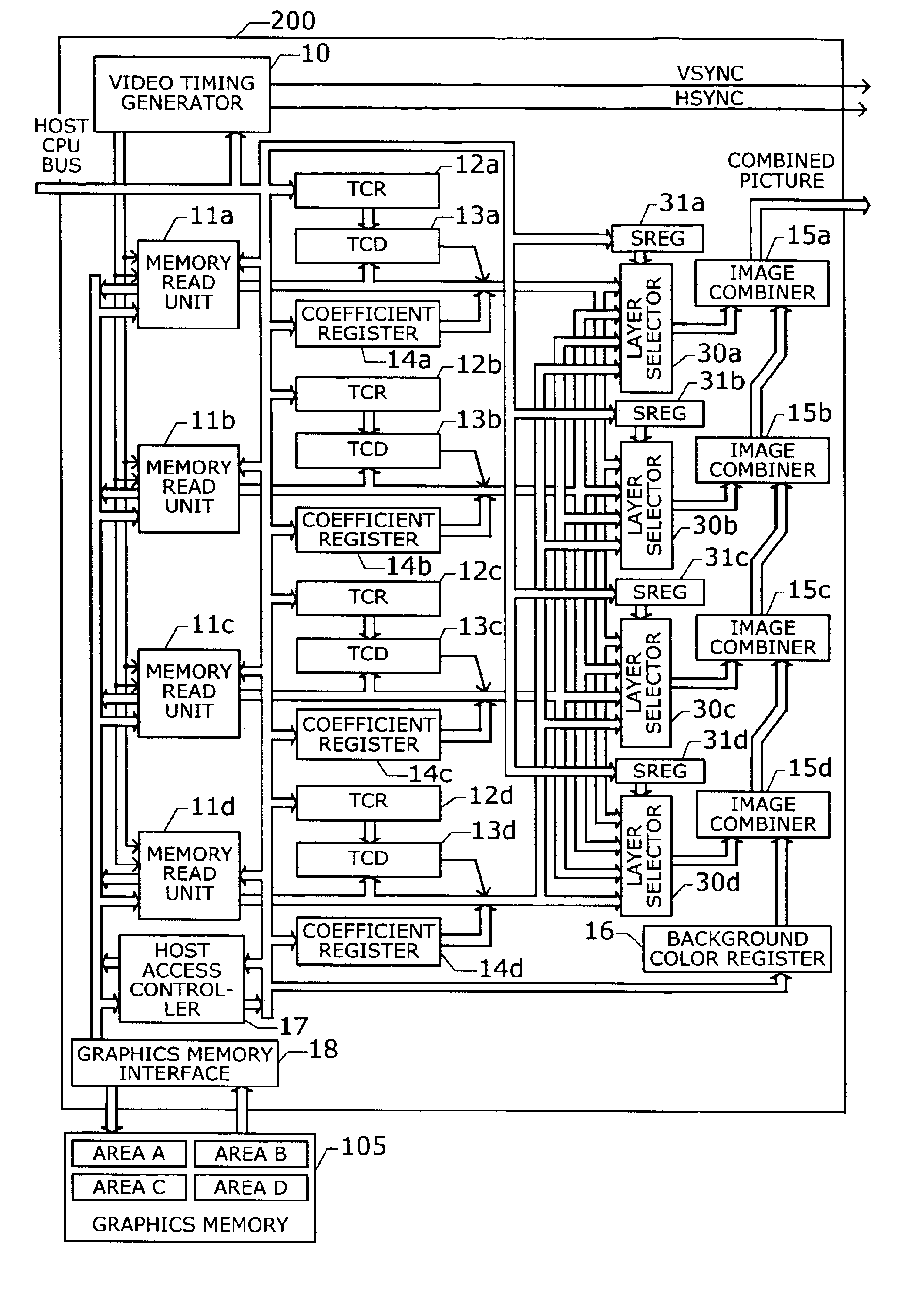
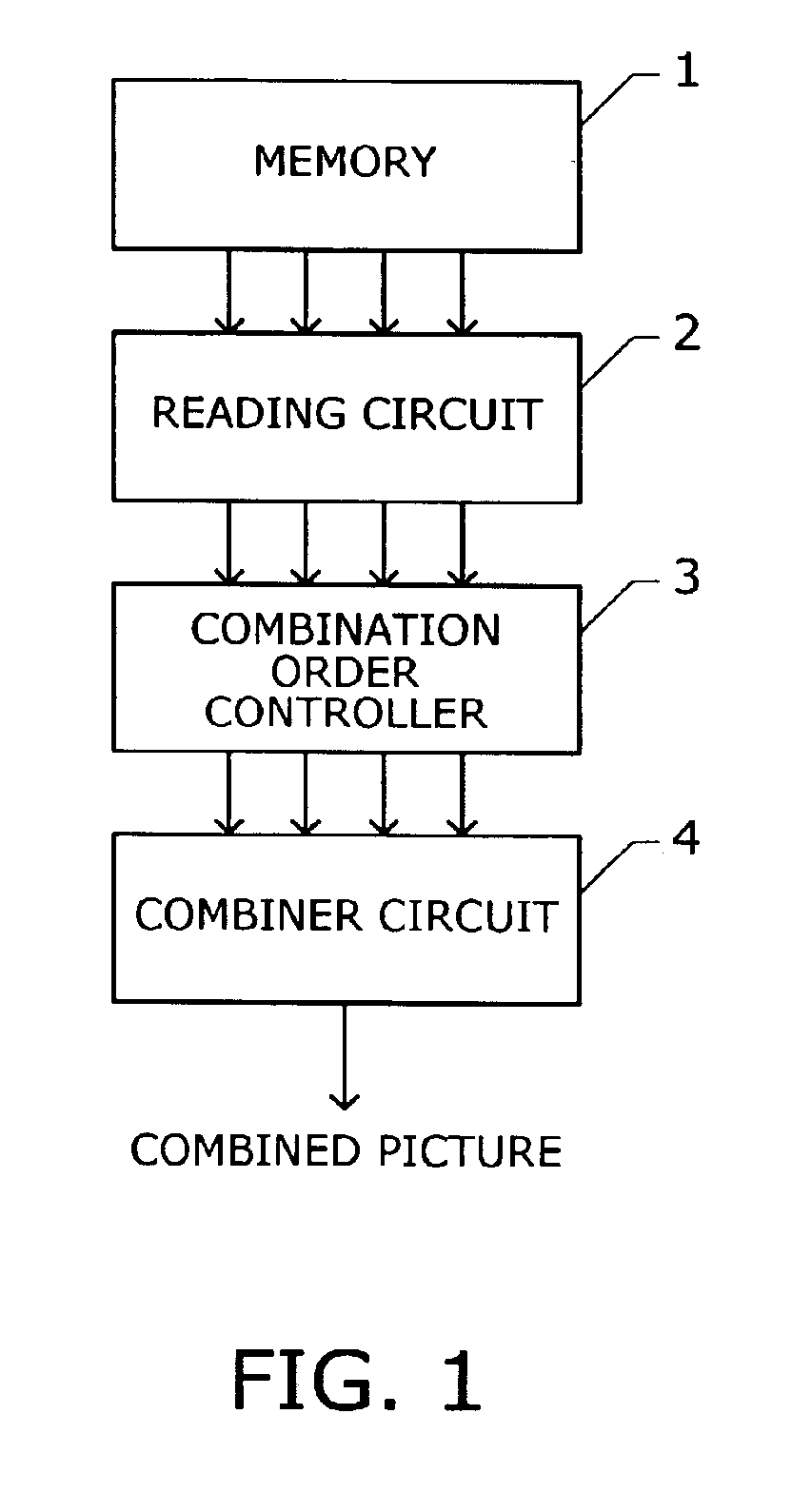
[0038]FIG. 1 is a conceptual view of the present invention. According to the present invention, the proposed image processing device comprises a memory 1, a reading circuit 2, a combination order controller 3, and a combiner circuit 4. The memory 1 has a plurality of predetermined storage areas each containing one layer of image data. The reading circuit 2 reads them out of the memory 1 as source images for a final picture. The combiner circuit 4 contains a plurality of image combiners cascaded one after another to combine the plurality of source images provided from the reading circuit 2 in a predetermined order. The combination order controller 3, disposed between the reading circuit and combiner circuit, determines which source image to supply to each image combiner, thereby controlling the orde...


PUM


Abstract

A graphics processing device and a semiconductor chip therefor, which offer a simple and easy way to change the order of layers in a combined picture. A reading circuit reads a plurality of source images out of a graphics memory. A combiner circuit combines given source images in a specific order. A combination order controller, disposed between the reading unit and combiner circuit, determines in what order the source images should be combined by the combiner circuit.

Description

CROSS REFERENCE TO RELATED APPLICATIONS[0001]This application is based upon and claims the benefits of priority from the prior Japanese Patent Application No. 2002-091652, filed on Mar. 28, 2002, the entire contents of which are incorporated herein by reference.BACKGROUND OF THE INVENTION[0002]1. Field of the Invention[0003]The present invention relates to an image processing device for layered graphics and a semiconductor chip implementing that device. More particularly, the present invention relates to an image processing device, as well as to a semiconductor integrated circuit chip, which reads out a plurality of source images from a graphics memory and combines them in a predetermined order to form a single picture.[0004]2. Description of the Related Art[0005]Graphics functions employed in some electronic devices, such as car navigation systems, take advantages of a multiple-layer structure of graphics data, where a picture is represented as a set of overlaid images that are eac...

Claims


Application Information

Patent Timeline
Patent Type & Authority Patents(United States)
IPC IPC(8): G06G5/00G06T1/00G06T1/20G06T3/00G09G5/00G09G5/377G09G5/395H04N1/387
CPCG09G5/397G09G2340/10
Inventor KOMAGATA, YOSHINOBU
Owner INTELLECTUAL VENTURES I LLC
Why Eureka
Try Eureka