Method for providing clock-net aware dummy metal using dummy regions

a clocknet aware and dummy metal technology, applied in the field of patterning dummy metal, can solve the problems of degrading the overall performance of the integrated circuit, less available space in each tile for dummy metal insertion, and increasing the capacitance between the dummy lines and the signal wires, so as to minimize the timing impact of adjacent clock nets

Active Publication Date: 2006-02-28
BELL SEMICON LLC
View PDF7 Cites 15 Cited by
  • Summary
  • Abstract
  • Description
  • Claims
  • Application Information

AI Technical Summary

Benefits of technology

[0011]According to the method and system disclosed herein, inserting dummy metal into dummy regions that are not adjacent to clock nets prior to inserting dummy metal into clock-net adjacent dummy regions will be sufficient to meet the minimum density requirement. This means that in many cases, no dummy metal (or a minimal amount) is inserted in the clock-net adjacent dummy regions, thereby minimizing the timing impact to the adjacent clock nets.

Problems solved by technology

That is, patterning the dummy metal too close to signal nets increases capacitance between the dummy lines and the signal wires.
The increased capacitance can affect the signal nets by slowing the transmission speed of signals, thereby degrading overall performance of the integrated circuit.
However, hardcoding a large “stay-away” distance between dummy metal and clock nets may lead to less available space in each tile for dummy metal insertion.
In this scenario, use of the simple large dummy-to-clock distance methodology is disadvantageous.
This is because it is often impossible to insert enough dummy metal into a tile to meet the required minimum density without reducing the large dummy-to-clock distance.
Such an involved, iterative process can significantly impact the design schedule.

Method used


Image

  • Method for providing clock-net aware dummy metal using dummy regions
  • Method for providing clock-net aware dummy metal using dummy regions
  • Method for providing clock-net aware dummy metal using dummy regions

Examples


Embodiment Construction

[0018]The present invention relates to design methodologies for dummy metal filling. The following description is presented to enable one of ordinary skill in the art to make and use the invention and is provided in the context of a patent application and its requirements. Various modifications to the preferred embodiments and the generic principles and features described herein will be readily apparent to those skilled in the art. Thus, the present invention is not intended to be limited to the embodiments shown, but is to be accorded the widest scope consistent with the principles and features described herein.

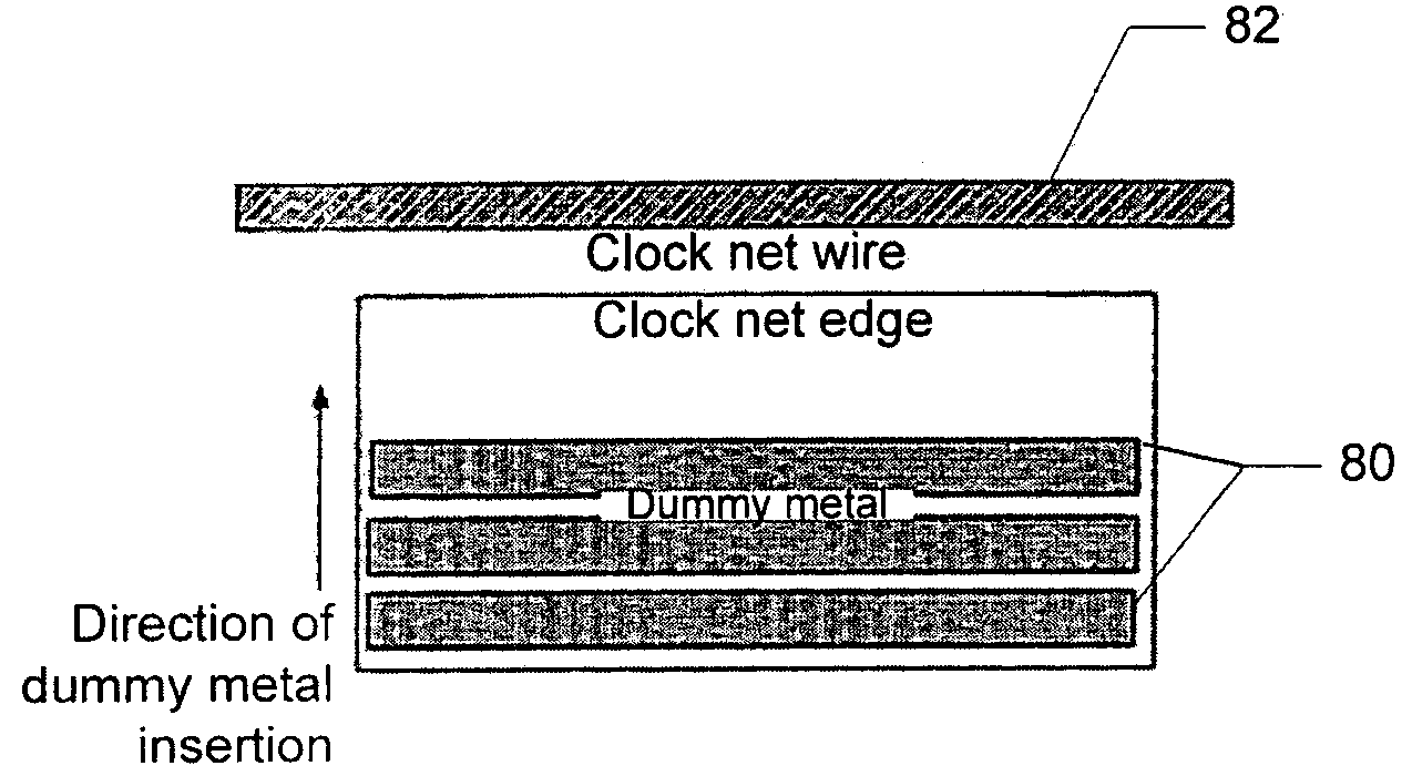
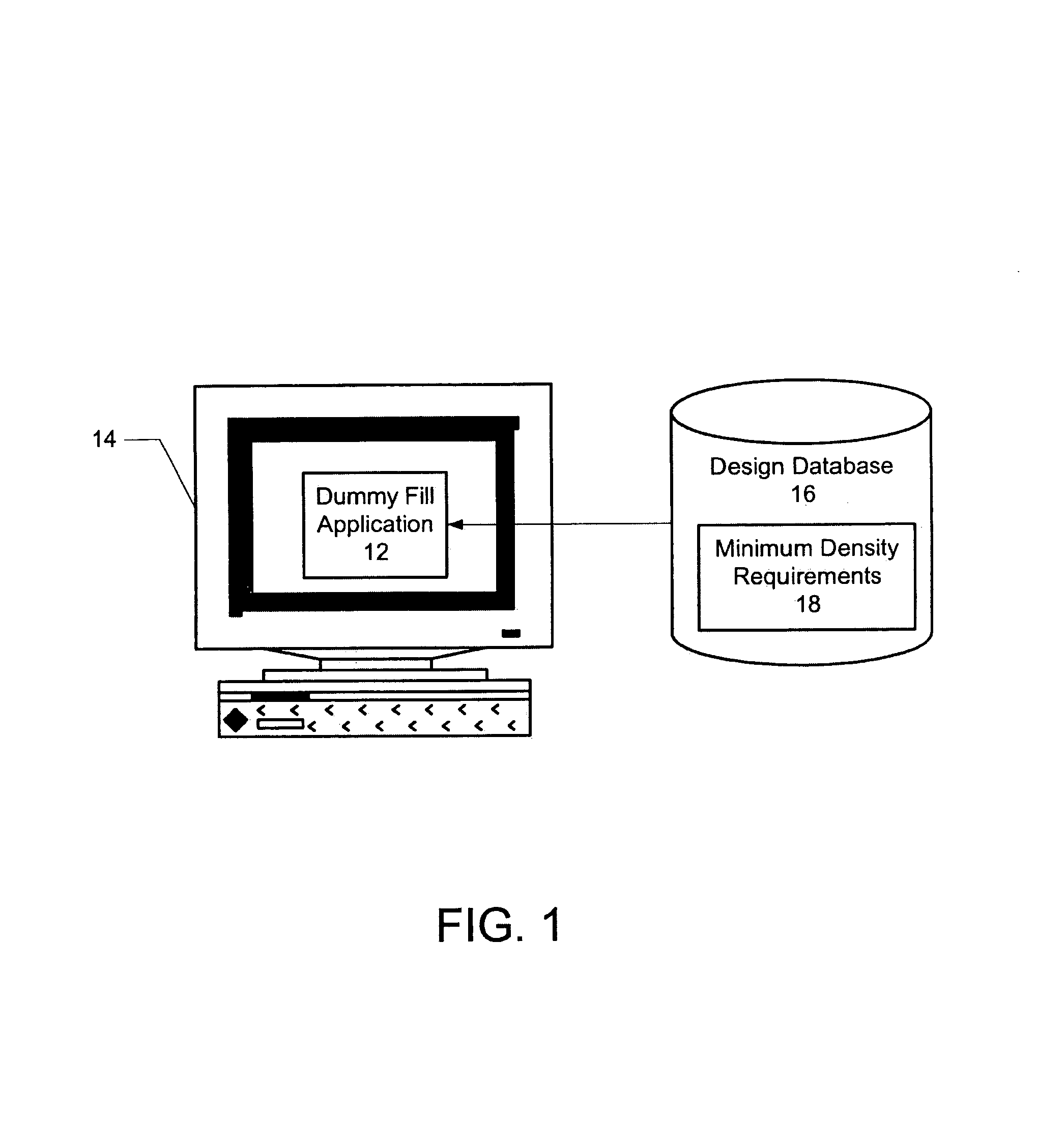
[0019]The present invention provides a software tool for dummy metal filling of a chip design during the design phase. FIG. 1 is a block diagram illustrating a software and hardware environment in which the present invention may be implemented. The dummy fill software application 12 is preferably executed on a computer 14, which may be a workstation or a server. The dummy fi...


PUM


Abstract

A method and system is disclosed for inserting dummy metal into a circuit design, which includes a plurality of objects and clock nets. Aspects of the invention include identifying free spaces on each layer of the chip design suitable for dummy metal insertion, wherein the free spaces are referred to as dummy regions. Thereafter, the dummy regions are prioritized such that the dummy regions located adjacent to clock nets are filled with dummy metal last. In a preferred embodiment, the dummy regions are further prioritized such that the dummy regions adjacent to wider clock nets are filled with dummy metal after dummy regions that are located adjacent to narrower clock nets.

Description

FIELD OF THE INVENTION[0001]The present invention relates to methods for patterning dummy metal to achieve planarity for chemical-mechanical polishing of integrated circuits, and more particularly to a dummy fill software tool that provides clock-net aware dummy metal using dummy regions.BACKGROUND OF THE INVENTION[0002]Chemical Mechanical Polishing (CMP) is a part of the chip fabrication process that requires a uniform distribution of metal and silicon over the surface of the chip. To achieve this distribution, pieces of interconnect (metal or silicon) must be inserted into available spaces in low-density regions of the chip. This interconnect insertion is called dummy metal filling or simply dummy filling, and the inserted interconnect is called dummy metal.[0003]Most fabrication processes require a minimum density for the interconnects on each layer of a multi-layer chip design. The interconnect density for a region is the sum total of the area of all interconnect in that region ...

Claims


Application Information

Patent Timeline
Patent Type & Authority Patents(United States)
IPC IPC(8): G06F9/45G06F17/50
CPCG06F17/5068G06F2217/62G06F2217/12G06F30/396G06F2119/18G06F30/39Y02P90/02G06F30/398
Inventor SHROWTY, VIKRAMRAMAN, SANTHANAKRISHNAN
Owner BELL SEMICON LLC
Why Eureka
Try Eureka