FPGA blocks with adjustable porosity pass thru

a technology of porosity and gate array, applied in logic circuits using specific components, instruments, semiconductor/solid-state device details, etc., can solve the problems of inability to wire through the chip in the macro area, channel blockage, and inability to meet the requirements of micro-controllers, so as to minimize the chip floor plan and timing impact

Inactive Publication Date: 2005-06-09
IBM CORP
View PDF2 Cites 6 Cited by
  • Summary
  • Abstract
  • Description
  • Claims
  • Application Information

AI Technical Summary

Benefits of technology

[0014] The invention also relates to a method for minimizing chip floor plan and timing impacts due to size growth of the FPGA. The method includes (a) assuming a fixed overall level of porosity for the whole core, and (b) allowing the ‘open’ wiring tracks to be shifted between the blocks as needed.

Problems solved by technology

This factor creates an inability to wire through the chip in the area of the macro.
These FPGAs are dense macros within the chip that require significant metal usage, often resulting in unacceptable wiring blockage such that key, timing critical wires must be routed around the macro, resulting in unacceptable timing delays.
Due to the significant usage of metal layers in FPGA circuitry, channels are blocked when the arrays are embedded in the chip.
This can cause unacceptably long signal delays impacting overall chip performance and reliability because of the longer circuit paths.
One solution would be to place uniform wiring channels at regular intervals through an FPGA during the macro's design but, depending upon the usage, there may be either too many wiring channels or not enough.
This is an inefficient use of the channels.

Method used


Image

  • FPGA blocks with adjustable porosity pass thru
  • FPGA blocks with adjustable porosity pass thru
  • FPGA blocks with adjustable porosity pass thru

Examples


Embodiment Construction

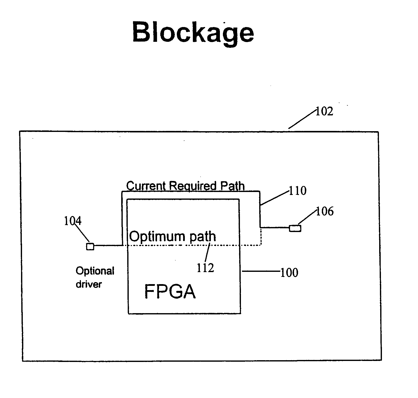
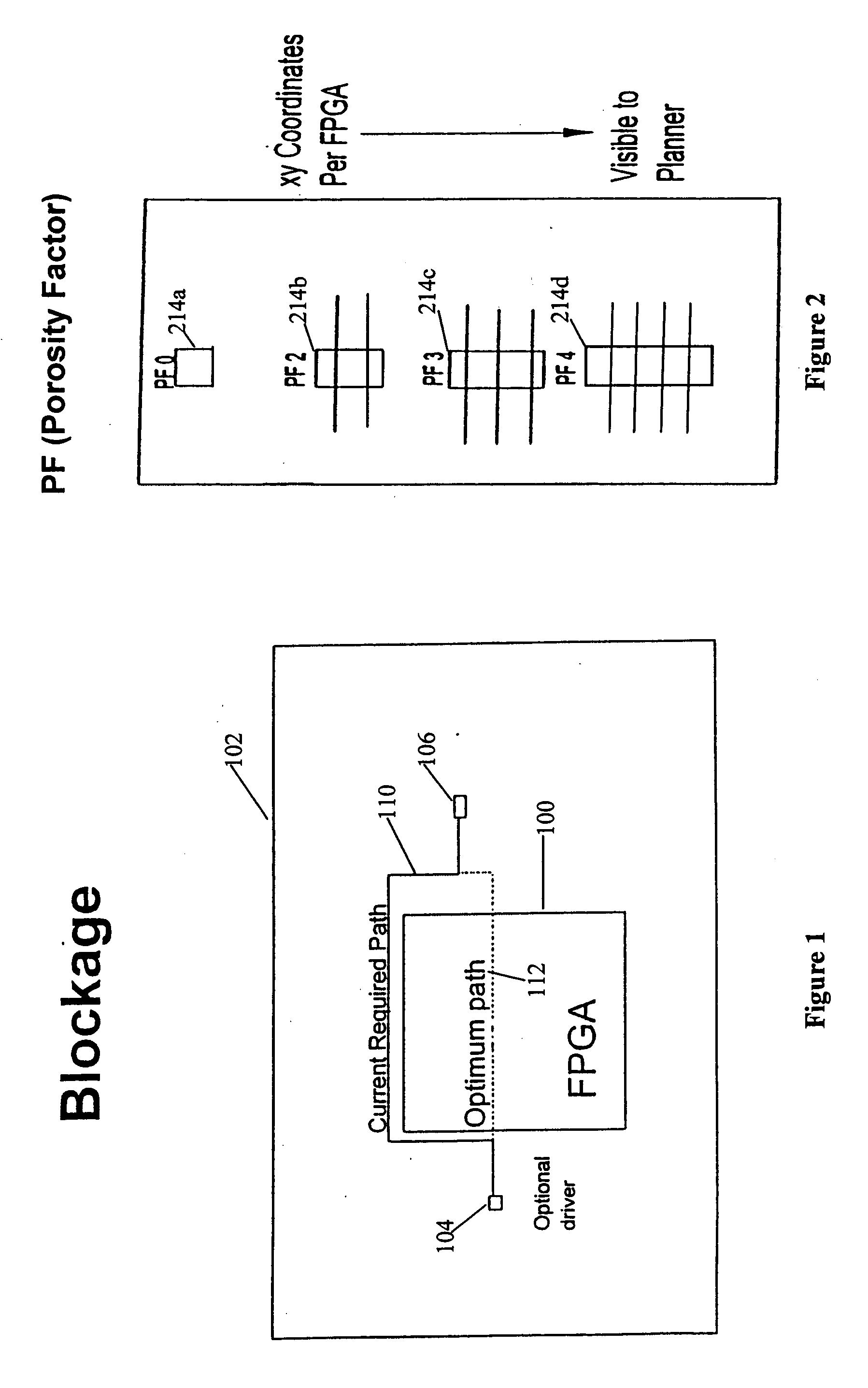
[0022] A VLSI chip includes a large number of electrical and logical functions, such as static and dynamic random access memory, read only storage, and programmable logic arrays. The chip is partitioned into regions that might contain different functions. The chip layout is designed to interconnect the different regions while keeping the interconnects as short as possible.

[0023] When custom designing a chip, there are certain requirements for the timing relationships between signals that go into the chip and the signals that exit the chip. Since the chip is very complex, the relationship of these I / O signals translates into a number of other requirements for the timing within the chip, and that go through circuits and that intersect certain storage elements within the chip. All of the timing requirements must be met for the chip to function properly within the system. These number in the hundreds of thousands of timing relationships that must interleave smoothly and must complement...


PUM


Abstract

A field programmable gate array is described for use in a semiconductor chip such as a VLSI chip. The array is provided with variable wire-through porosity to allow for optimum chip-level routing through the array. This is achieved by dividing the array into blocks which can be individually assessed for required porosity. Then blocks that have been prefabricated with differing porosities are placed in the macro to optimize local chip level routing. The routing of wires is determined by developing a chip floor plan to include early timing allocation and a proposed placement of the array. The floor plan is then overlaid with critical logical wiring nets. From this, an initial selection of blocks is made based on proposed wiring density, and the macro is assembled with the blocks strategically placed therein. The procedure is likewise applicable to other types of densely obstructed cores embedded with a chip.

Description

FIELD OF THE INVENTION [0001] This invention relates to the field gate array programming facility capable of efficiently and independently accessing logical blocks of physically local, as well as remotely distributed data, and to the method of making the same. BACKGROUND OF THE INVENTION [0002] For the last past two decades, integrated circuits have been composed of logical and physical units made of gating elements and wiring elements to interconnect the logic. There has been a trend toward larger stand-alone functional units called macros. These macros use a substantial silicon area on a semiconductor chip. One of the newer units is an embedded field programmable gate array (FPGA) macro. These macros use up a large area of a chip and a significant portion of the wiring channels that pass through the chip. This factor creates an inability to wire through the chip in the area of the macro. [0003] Currently, FPGAs are becoming an accepted component embedded within standard chip desig...

Claims


Application Information

Patent Timeline
Patent Type & Authority Applications(United States)
IPC IPC(8): H01L27/10H01L27/118H03K19/177
CPCH01L27/11803G06F17/5068G06F30/39
Inventor REYNOLDS, CHRISTOPHER B.VENTRONE, SEBASTIAN T.WEIL, ANGELA
Owner IBM CORP
Why Eureka
Try Eureka