Probing method and probing apparatus

a technology of probes and probes, applied in the direction of electronic circuit testing, measurement devices, instruments, etc., can solve the problems of inability to obtain constant contact load, possible wrong three-dimensional correction of the contact position of the probes, etc., and achieve high-accuracy inspection

Inactive Publication Date: 2006-03-07
TOKYO ELECTRON LTD
View PDF19 Cites 119 Cited by
  • Summary
  • Abstract
  • Description
  • Claims
  • Application Information

AI Technical Summary

Benefits of technology

[0013]An object of the present invention is to bring probes and electrode pads of an object of inspection accurately into contact with one another under a steady load even if a probe card is deformed from various causes or expanded or contracted by any thermal effect.
[0014]Another object of the of the invention is provide a probing method and a probing apparatus, in which probes and electrode pads of an object of inspection can be brought accurately into contact with one another if a main chuck is tilted by an unbalanced load during overdrive operation, so that high-accuracy inspection can be enjoyed.

Problems solved by technology

If the estimated load and an actual load are inconsistent, therefore, the three-dimensional correction of the contact position of the probes may possibly be wrong.
Since the overdrive of the main chuck is fixed, however, a constant contact load cannot be obtained.

Method used


Image

  • Probing method and probing apparatus
  • Probing method and probing apparatus
  • Probing method and probing apparatus

Examples


Embodiment Construction

[0082]A probing method and a probing apparatus according to the present invention can be used to check integrated circuits on a wafer for electrical properties. Alternatively, however, the invention may be applied to the inspection of the electrical properties of general electronic components such as LCD's.

[0083]In order to explain the present invention more specifically and definitely, there will be described a case in which the invention is applied to the inspection of the electrical properties of integrated circuits formed on a wafer.

[0084]The invention will be described in connection with embodiments shown in FIGS. 1 to 7, in which like reference numerals refer to like or equivalent portions throughout the several views.

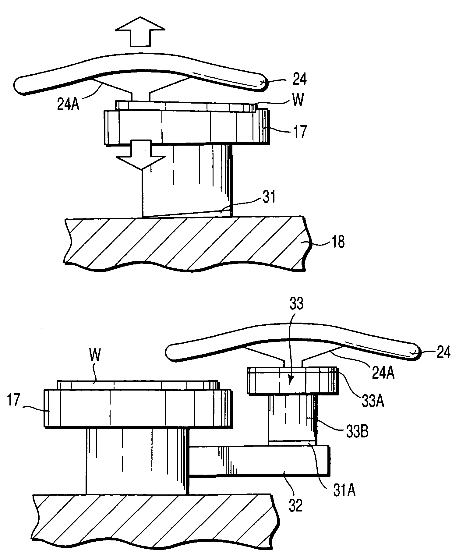
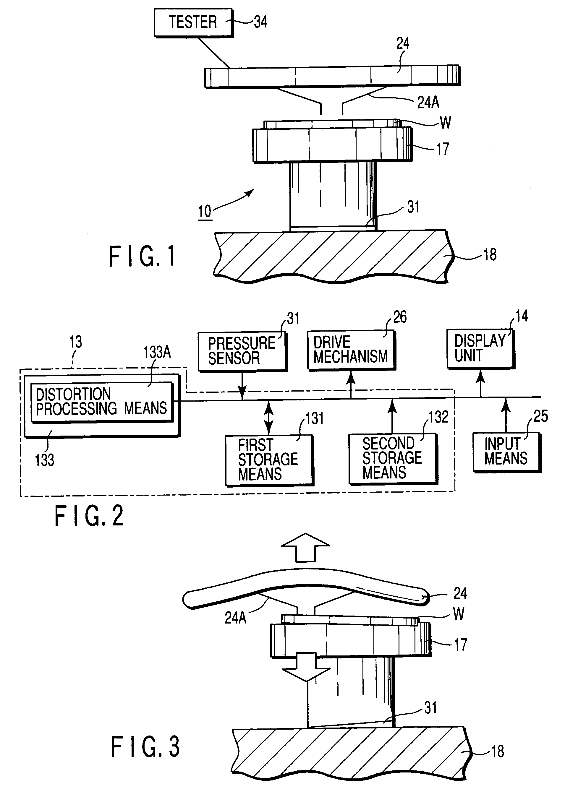
[0085]A probing apparatus 10 according to an embodiment of the invention, like the probing apparatus shown in FIG. 8, may be provided with a loading chamber 11 and a probing chamber 12. Alternatively, however, the loading chamber 11 and the probing chamber 12 may...


PUM


Abstract

Disclosed is a probing method comprising steps of moving a main chuck to align an object of inspection on the main chuck with probes of a probe card located over the main chuck, moving the main chuck toward the probe card, thereby bringing electrodes of the object of inspection into contact with the probes, overdriving the main chuck toward the probe card while measuring a load applied to the object of inspection by contact with the probes and controlling the movement of the main chuck in accordance with the measured load, and inspecting the electrical properties of the object of inspection by means of the probes.

Description

CROSS-REFERENCE TO RELATED APPLICATIONS[0001]This is a Continuation-in-Part application of U.S. patent application Ser. No. 09 / 667,502, filed Sep. 22, 2000 now U.S. Pat. No. 6,777,968, the entire contents of which are incorporated herein by reference.[0002]This application is based upon and claims the benefit of priority from the prior Japanese Patent Application No. 11-285139, filed Oct. 6, 1999, the entire contents of which are incorporated herein by reference.BACKGROUND OF THE INVENTION[0003]The present invention relates to a probing method and a probing apparatus, and more specifically, to a probing method and a probing apparatus with high reliability, in which a load applied to a main chuck carrying an object of inspection thereon by probes is measured when the main chuck is overdriven to the probes, so that a steady load can always be applied to the main chuck in accordance with the measured value.[0004]As shown in FIG. 8, a probing apparatus 10 for checking integrated circuit...

Claims


Application Information

Patent Timeline
Patent Type & Authority Patents(United States)
IPC IPC(8): G01R31/02G01R31/28
CPCG01R31/2887
Inventor KOBAYASHI, MASAHITOISHII, KAZUNARI
Owner TOKYO ELECTRON LTD
Why Eureka
Try Eureka