Assembly method of direct-docking probing device

a probing device and assembly method technology, applied in the field of probing devices, can solve the problems of increased cost burden on users, possible signal failure, and higher unit cost of the probe interface board b>12/b>, and achieve the effect of accurate conta

Active Publication Date: 2015-02-05
MICROELECTRONICS TECH INC
View PDF4 Cites 18 Cited by
  • Summary
  • Abstract
  • Description
  • Claims
  • Application Information

AI Technical Summary

Benefits of technology

[0024]Because the mechanical strength of the reinforcing plate is larger than that of the space transforming plate, the amount of deformation of the reinforcing plate is smaller than that of the space transforming plate. Therefore, the offset amount of the vertical probe assembly is small, so that the vertical probes can be more accurately contacted with the device under test.

Problems solved by technology

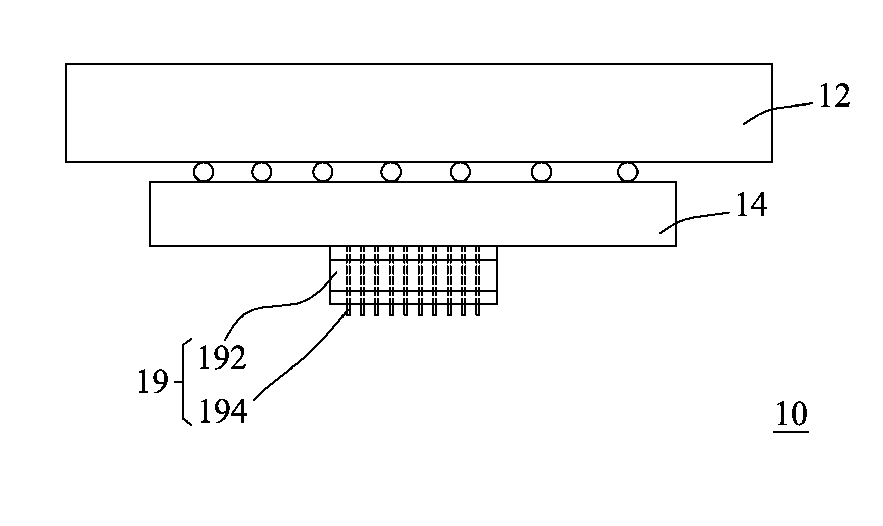
Because the signal transmission path is of a relatively long distance, signal failure is possible to occur when a plurality of high-frequency test signals are transmitted.
In addition, the unit cost of the probe interface board 12 is higher due to having more electronic components disposed thereon, and the cost burden on the user is thereby increased.
However, the height from the bottom surface of the probe interface board 22 to the tip of the vertical probe assembly 29 is limited by the usage environment; thus, such height is harder to be adjusted when the space transforming plate 24 becomes thinner.
Therefore, the probes of the vertical probe assembly 29 cannot accurately be contacted with the device under test.

Method used


Image

  • Assembly method of direct-docking probing device
  • Assembly method of direct-docking probing device
  • Assembly method of direct-docking probing device

Examples


second embodiment

[0053]Please refer to FIG. 4C which shows a probing device 30′ of a second embodiment in the present invention. In the probing device 30′, the solders 342 are surrounded by a filler layer 344, and the filler layer 344 is made of polymer material. The filler layer 344 is used to prevent the solders 342 from being polluted by the external environment. Because the other elements of the probing device 30′ is identical or similar to the elements shown in FIG. 4B, they are marked with the same numbers in FIG. 4C and not described in detail.

[0054]Person of ordinary skill in the art can use other protective device to replace the protective spacer 37, for example: a protective frame. The protective frame is a hollow plate-shaped object and is located around the conductive elastic member 36. The hollow portion of the protective frame is used to contain the conductive elastic member 36. The two ends of the protective frame are pressed on the probe interface board 32 and the reinforcing plate 3...

third embodiment

[0058]Please refer to FIG. 6 which shows a probing device 40 of a third embodiment in the present invention. The probing device 40 includes two protective screws 47. The protective screws 47 are penetrated through the probe interface board 32, and the bottom ends of the protective screws 47 are pressed on the reinforcing plate 343. The protective screws 47 and the protective spacer 37 have a similar function, i.e. preventing the space transformer 34 from being deflected toward the probe interface board 32, so as to avoid the electrical contacts 364 being compressed and damaged. The assembly method of the probing device 40 is similar to that of the probing device 30, and the difference is that after the fixing frame 35 is mounted on the probe interface board 32, the protective screws 47 are screwed so as to make its end being pressed on the reinforcing plate 343.

fourth embodiment

[0059]Please refer to FIG. 7 which shows a probing device 50 of a fourth embodiment in the present invention. In the probing device 50, a limit portion 3541′ is formed on the frame body 354′ of the fixing frame 35′. Compared with respect to the holding portion 356, the limit portion 3541′ is holding on the other side of the reinforcing plate 343. In other words, the reinforcing plate 343 is clamped by the holding portion 356 and the limit portion 3541′. Because of the limit portion 3541′, the deformation of the space transformer 34 caused by the reaction force from the device under test can be avoided. In addition, the limit portion 3541′ can prevent the transformer 34 from being deflected toward the probe interface board 32 and protect the electrical contacts 364 from being compressed and damaged, so that the limit portion 3541′ can be a protective device for the probing device 50. The assembly method of the probing device 50 is similar to that of the probing device 30, and thus no...


PUM

PropertyMeasurementUnit
thicknessaaaaaaaaaa
thicknessaaaaaaaaaa
thicknessaaaaaaaaaa

Abstract

An assembly method of direct-docking probing device is provided. First, a space transforming plate made by back-end-of-line semiconductor manufacturing process is provided, so the thickness of the space transforming plate is predetermined by the client of probe card manufacturer. Then a reinforcing plate in which a plurality of circuits disposed is provided, which has larger mechanical strength than the space transforming plate. After that the reinforcing plate and the space transforming plate are joined and electrically connected by a plurality of solders so as to form a space transformer. Then, a conductive elastic member and a probe interface board are provided. Thereafter, the space transformer and the conductive elastic member are mounted on the probe interface board. After that, at least one vertical probe assembly having a plurality of vertical probes is mounted on the space transforming plate, and the vertical probes is electrically connected with the space transforming plate.

Description

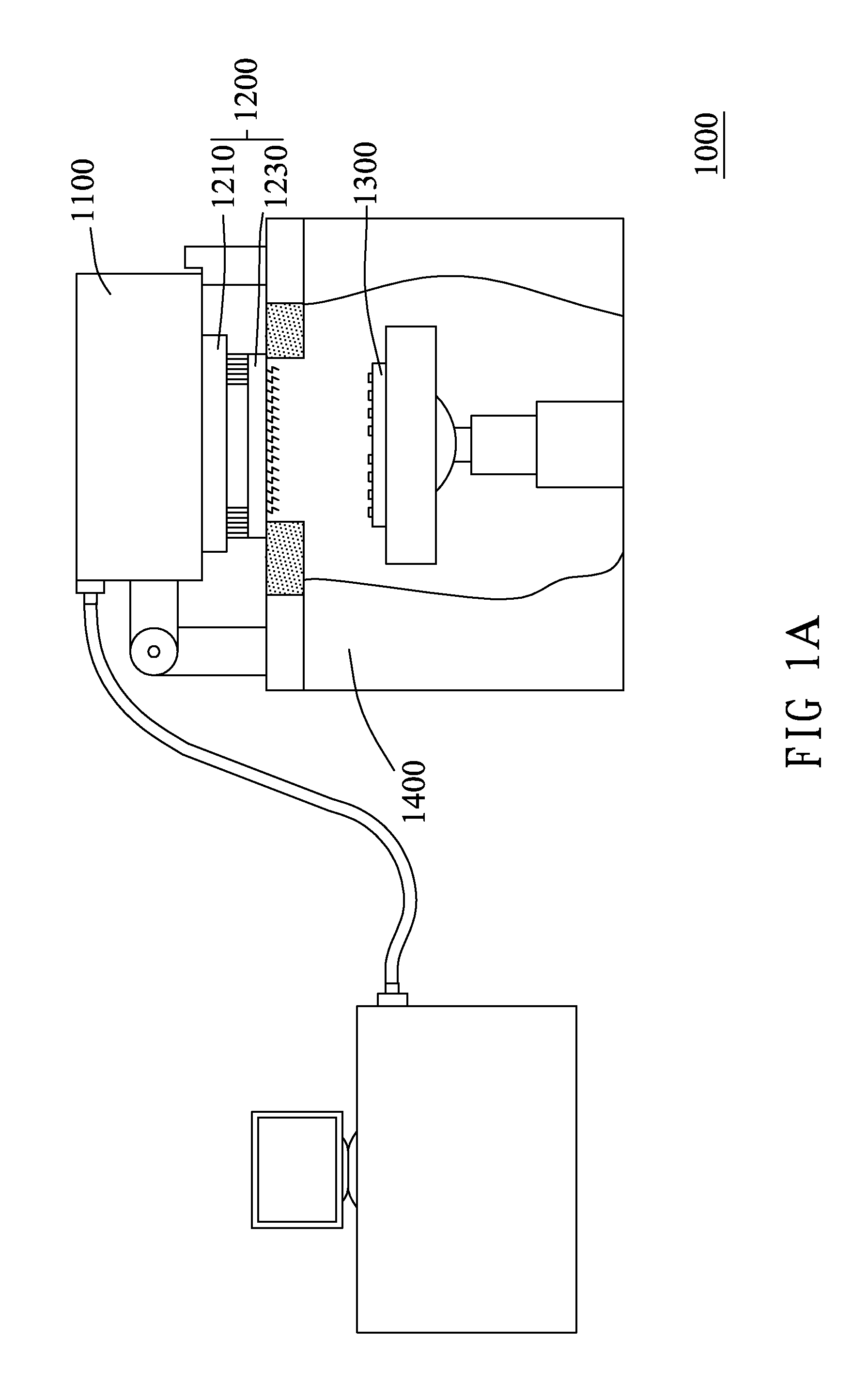
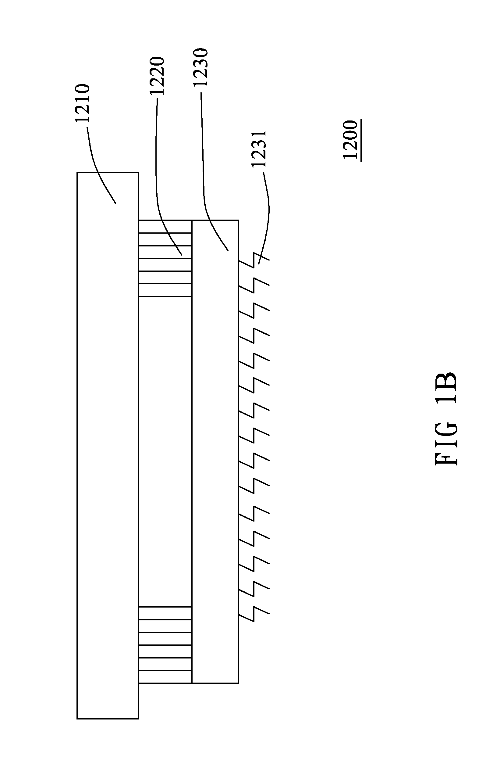
CROSS-REFERENCE TO RELATED APPLICATION [0001]This application is a non-provisional continuation-in-part application claiming priority of U.S. non-provisional application Ser. No. 13 / 091,148, filed on Apr. 21, 2011, which is currently pending. The entirety of the above-mentioned patent application is hereby incorporated by reference herein and made a part of this specification.FIELD OF INVENTION [0002]The invention relates to a probing device, especially relates to a probing device having a longer service life and a space transforming plate thereof to be less likely to be deformed.BACKGROUND OF THE INVENTION [0003]Please refer to FIG. 1A and FIG. 1B. FIG. 1A shows a conventional probing system. FIG. 1B shows a probing device shown in FIG. 1A. The probing system 1000 includes a test head 1100, a conventional probing device 1200, and a prober 1400. The probing device 1200 includes a probe interface board 1210, a pogo tower 1220, and a probe card 1230. The probing device 1200 is mounted...

Claims


Application Information

Patent Timeline
Patent Type & Authority Applications(United States)
IPC IPC(8): G01R3/00G01R31/28
CPCG01R3/00G01R31/2889G01R31/2887Y10T29/49128Y10T29/49204Y10T29/49004Y10T29/49208Y10T29/49222Y10T29/49155B23K2103/42G01R31/2853
Inventor WU, CHIEN-CHOUCHEN, MING-CHICHEN, TSUNG-YILI, CHUNG-CHE
Owner MICROELECTRONICS TECH INC
Why Eureka
Try Eureka