EL display device and manufacturing method thereof

a technology of polarization film and manufacturing method, applied in the direction of discharge tube luminescnet screen, identification means, instruments, etc., can solve the problems of increased manufacturing costs, inability to extract light emitted from the luminescing layer, and high cost of polarization film

Inactive Publication Date: 2006-03-14
SEMICON ENERGY LAB CO LTD
View PDF6 Cites 14 Cited by
  • Summary
  • Abstract
  • Description
  • Claims
  • Application Information

AI Technical Summary

Benefits of technology

[0010]The present invention is made in view of the above problems, and an object of the present invention is to prevent an EL display device from becoming mirrored, and to provide a low cost EL display device in which the EL display device manufacturing cost has been reduced. In addition, an object of the present invention is to lower the cost of an electronic device having a display using the EL display device.
[0014]Further, by forming projecting portions in other thin films contacting the cathode, and then forming the cathode on top, the projecting portion can be formed in the reflecting surface of the cathode. In particular, Japanese Patent Application Laid-open No. Hei 9-69642 and Japanese Patent Application Laid-open No. Hei 10-144927 can be cited for means of forming the projecting portion in an aluminum film. Namely, by forming the aluminum film based on the above patent applications, and by laminating the cathode on top of the aluminum film, it is possible to obtain a cathode having the projecting portion.

Problems solved by technology

This is done because if one of the pair of electrodes is not transparent, the light emitted from the luminescing layer cannot be extracted.
In order to avoid this, a method of attaching a circular polarization film to the EL display device so that the observer's face is not reflected is employed, but there is a problem in that the circular polarization film is extremely high cost, therefore leading to increased manufacturing costs.

Method used


Image

  • EL display device and manufacturing method thereof
  • EL display device and manufacturing method thereof
  • EL display device and manufacturing method thereof

Examples


embodiment mode 1

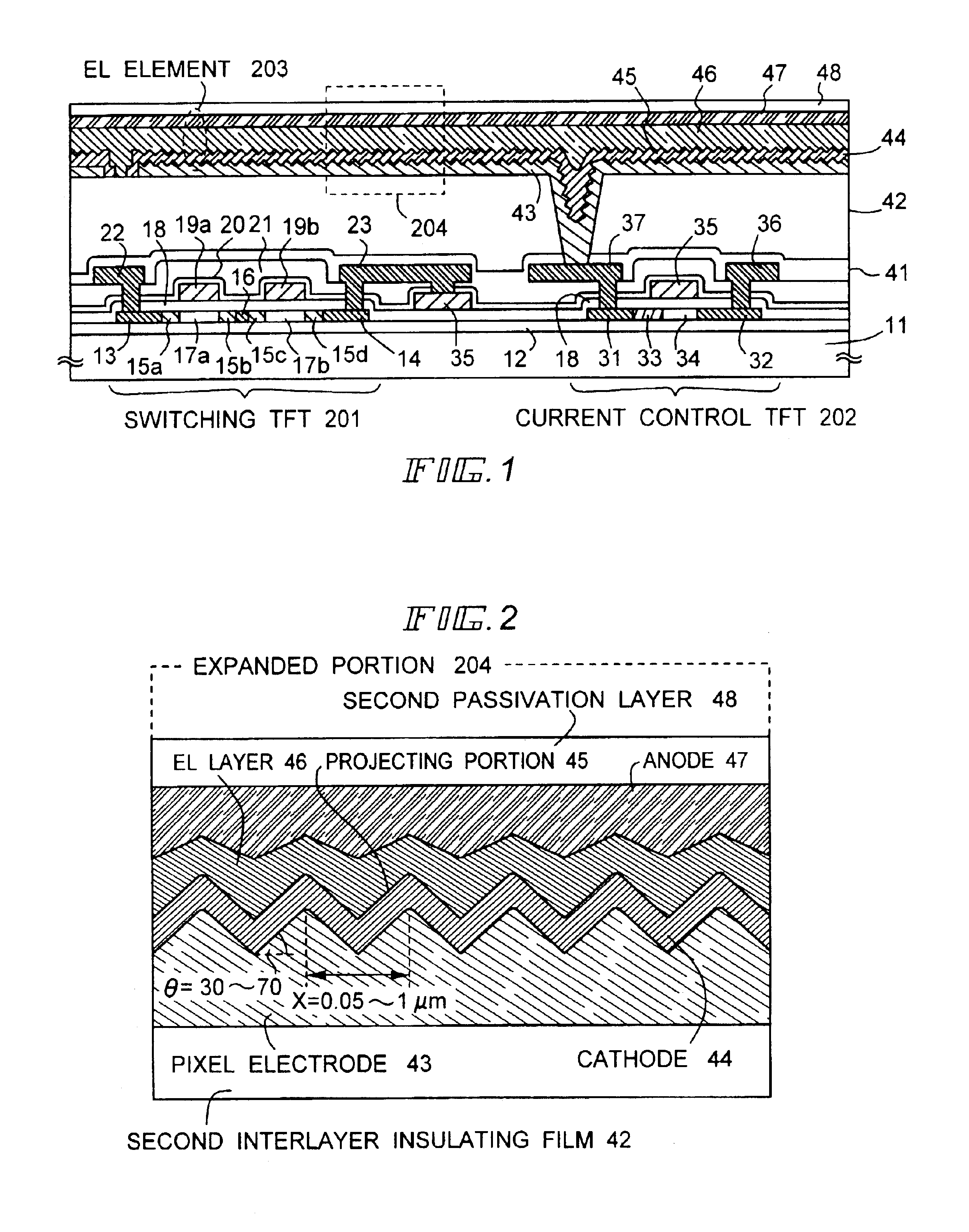
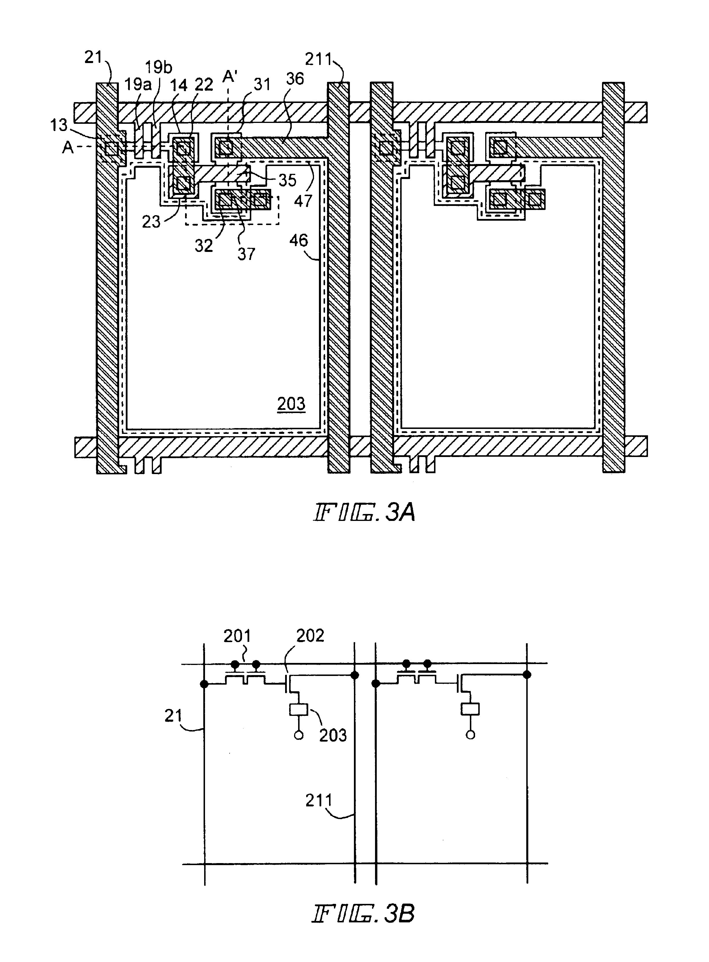
[0035]Embodiment mode 1 of the present invention will be explained using FIGS. 1 to 3B. Shown in FIG. 1 is a cross sectional diagram of a pixel portion of an EL display device of the present invention, while FIG. 2 shows an enlargement of a portion of FIG. 1. FIG. 3A is a top view of the EL display device, and FIG. 3B is a circuit diagram of the EL display device. In practice, a plurality of pixels arranged in a matrix shape is formed as the pixel portion (image display portion). Note that common symbols are used in FIGS. 1 to 3B, and therefore each of the diagrams may be suitably referred to. Further, two pixels are shown in the top view of FIG. 3A, but both have the same structure, and therefore only one is explained.

[0036]In FIG. 1, a reference numeral 11 designates a substrate; and 12, an insulating film (hereinafter referred to as an under film) which becomes an undercoat. A glass substrate, a glass ceramic substrate, a quartz substrate, a silicon substrate, a ceramic substrate...

embodiment mode 2

[0076]An example of using the present invention in a simple matrix type EL display device is shown in FIG. 16 in embodiment mode 2. In FIG. 16, reference numeral 1601 denotes a substrate, reference numerals 1602a denote aluminum films with added silicon, and 1602b are cathodes made from lithium fluoride films formed in succession on the aluminum films 1602a. Electrodes 1602 composed of these films in lamination are formed aligned in a stripe shape. The electrodes 1602 are referred to as first electrodes here.

[0077]In embodiment mode 2, the aluminum films 1602a are deposited so as to have projecting portions formed in their surfaces due to steps at the time of film deposition, and projecting portions 1603 are formed in the surface of the lithium fluoride film cathodes 1602b along the projecting portions formed in the base film aluminum films 1602a.

[0078]An EL layer 1604 is formed by a low molecular weight organic material or a high molecular weight organic material on the electrodes...

embodiment 1

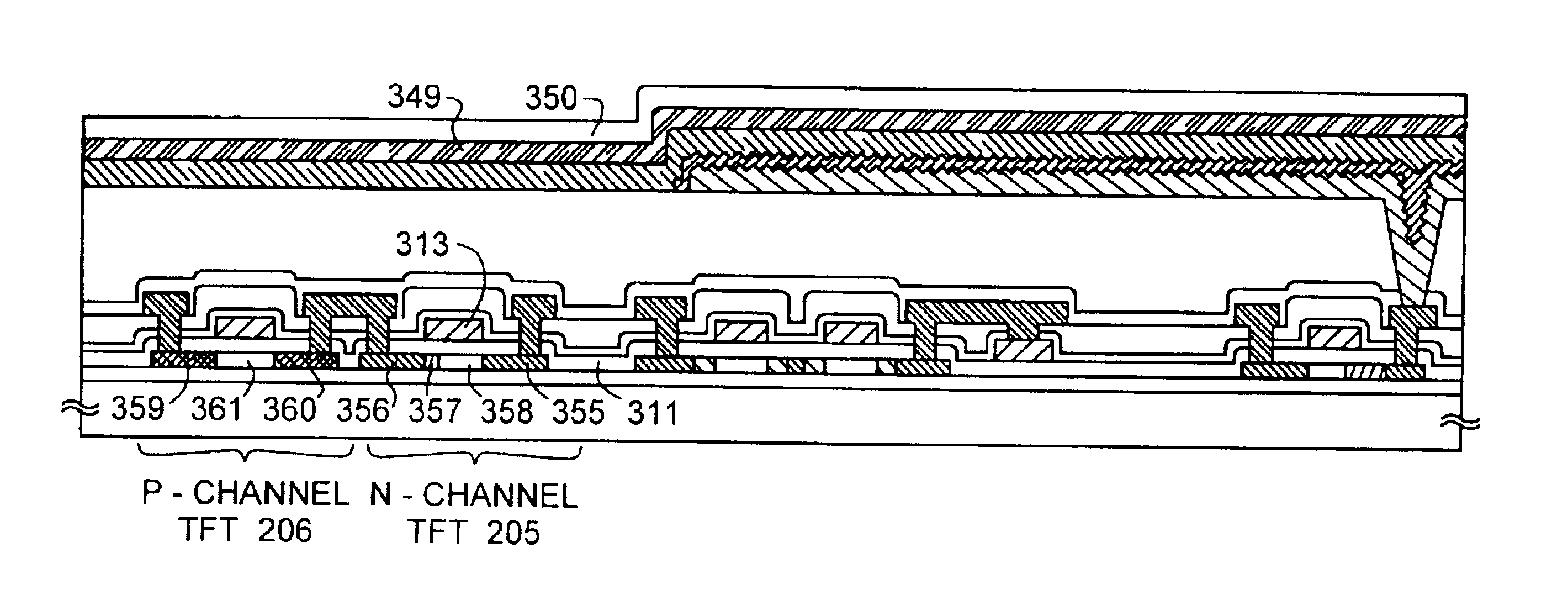
[0081]The embodiments of the present invention are explained using FIGS. 4A to 6C. A method of simultaneous manufacture of a pixel portion, and TFTs of a driver circuit portion formed in the periphery of the pixel portion, is explained here. Note that in order to simplify the explanation, a CMOS circuit is shown as a basic circuit for the driver circuits.

[0082]First, as shown in FIG. 4A, a base film 301 is formed with a 300 nm thickness on a glass substrate 300. Oxidized silicon nitride films are laminated as the base film 301 in embodiment 1. It is good to set the nitrogen concentration at between 10 and 25 wt % in the film contacting the glass substrate 300.

[0083]Besides, as a part of the under film 301, it is effective to provide an insulating film made of a material similar to the first passivation film 41 shown in FIG. 2. The current controlling TFT is apt to generate heat since a large current is made to flow, and it is effective to provide an insulating film having a heat rad...


PUM


Abstract

Reducing the manufacturing cost of an EL display device and an electronic device furnished with the EL display device is taken as an objective. A textured structure in which projecting portions are formed on the surface of a cathode is used. External stray light is diffusely (irregularly) reflected by the action of the projecting portions when reflected by the surface of the cathode, and therefore a defect in which the face of an observer or the surrounding scenery is reflected in the surface of the cathode can be prevented. This can be completed without using a conventionally necessary high price circular polarizing film, and therefore it is possible to reduce the cost of manufacturing the EL display device.

Description

[0001]This application is a continuation of U.S. application Ser. No. 10 / 186,398, filed on Jul. 1, 2002 now U.S. Pat. No. 6,555,967, which is a continuation of U.S. application Ser. No. 09 / 644,429, filed on Aug. 23, 2000, now U.S. Pat. No. 6,433,487 Aug. 13, 2002.BACKGROUND OF THE INVENTION[0002]1. Field of the Invention[0003]The present invention relates to an electro-optical device, typically an EL (electroluminescence) display device, and an electronic device (electronic equipment) having the electro-optical device as a display.[0004]2. Description of the Related Art[0005]The development of electro-optical devices, typically EL (electroluminescence) display devices using organic material for electroluminescence, has been proceeding at a rapid pace in recent years. There are two types of EL display devices, passive matrix type EL display devices and active matrix type EL display devices.[0006]Regardless of whether a passive matrix type or an active matrix type, the EL display devi...

Claims


Application Information

Patent Timeline
Patent Type & Authority Patents(United States)
IPC IPC(8): G09F9/30H01L29/76H05B44/00H01J1/62H01L27/32H01L31/12H01L51/50H01L51/52H05B33/02H05B33/10H05B33/12H05B33/14H05B33/26
CPCH01L27/3281H01L51/5206H01L51/5221H01L51/5231H01L51/5281H01L51/5203H01L27/1214H01L27/3244H01L29/78621H01L29/78627H01L2251/5315H01L51/5268H01L27/1251H10K59/123H10K59/17H10K59/12H10K50/81H10K50/822H10K50/826H10K50/854H10K50/86H10K2102/3026H10K2102/321H10K59/805H10K50/805H10K50/82H10K50/11
Inventor YAMAZAKI, SHUNPEI
Owner SEMICON ENERGY LAB CO LTD
Why Eureka
Try Eureka