Testing device for printed circuit boards

a testing device and printed circuit board technology, applied in the testing of individual semiconductor devices, detecting faulty computer hardware, instruments, etc., can solve the problems of low work efficiency, labor-intensive and easy to be misoperated, etc., and achieve the effect of having an overall test on the untested printed circuit board easily and quickly

Inactive Publication Date: 2006-03-21
HON HAI PRECISION IND CO LTD
View PDF5 Cites 9 Cited by
  • Summary
  • Abstract
  • Description
  • Claims
  • Application Information

AI Technical Summary

Benefits of technology

[0010]A principal advantage of this embodiment is that the testing device can have an overall test on the untested printed circuit board easily and quickly.

Problems solved by technology

However, there are so many elements on the printed circuit board, it is time-consuming to connect the footprints of the chips and slots with the terminals one by one by the operators, and it is labor-consuming and prone to misoperation.
However the testing device for CPU detection is only capable of the CPU testing, while the tests on the audio, the battery are ignored or have to be tested in another testing device.
The unqualified audio elements and the unqualified battery bring a lot of inconvenience to the users and the respective testing is labor-consuming and lead to low work efficiency.

Method used


Image

  • Testing device for printed circuit boards
  • Testing device for printed circuit boards
  • Testing device for printed circuit boards

Examples


Embodiment Construction

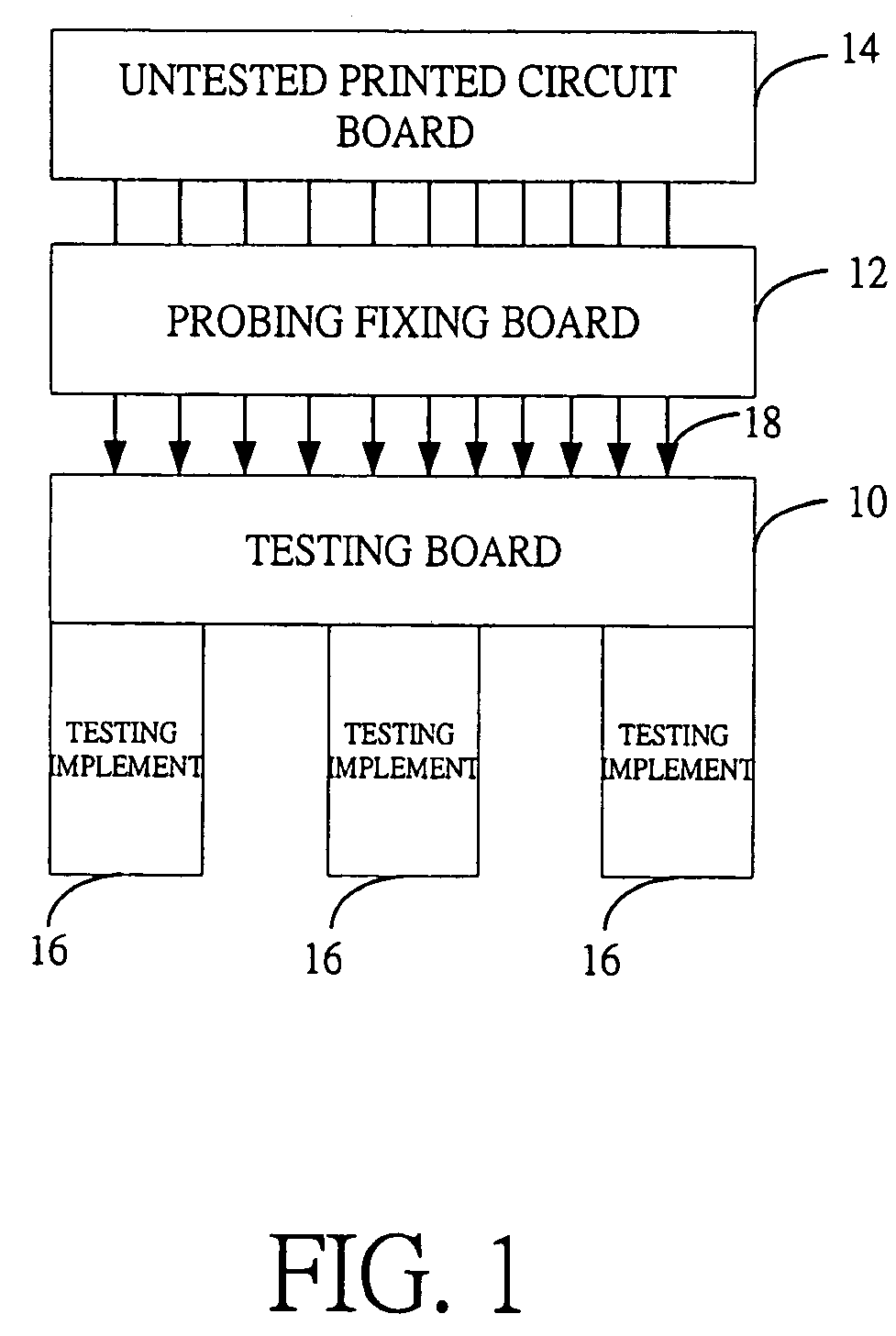
[0019]Referring to FIG. 1, a testing device for printed circuit boards is capable of detecting all kinds of functions of an untested printed circuit board 14 and outputting testing signals via a probing fixing board 12. The probing fixing board 12 comprises a plurality of probes 18. When testing, the probing fixing board 12 is put between the untested printed circuit board 14 and the testing board 10, and outputs the testing signals from the untested printed circuit board 14 to the testing board 10 via the probes 18. These testing signals are transferred to a plurality of testing implements 16 by the testing board 10. The testing implements 16, such as displays, instruments, analyze the testing signals and show the states as well as the results thereof.

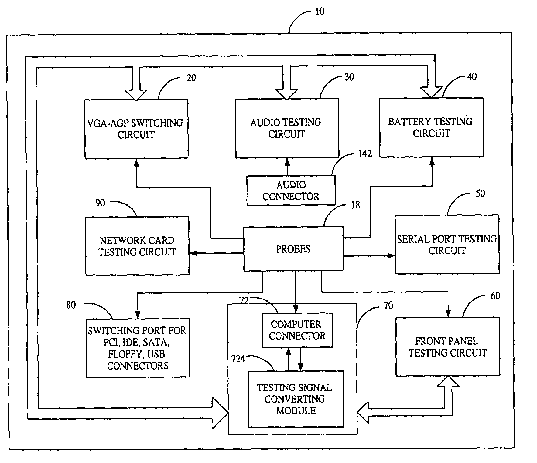
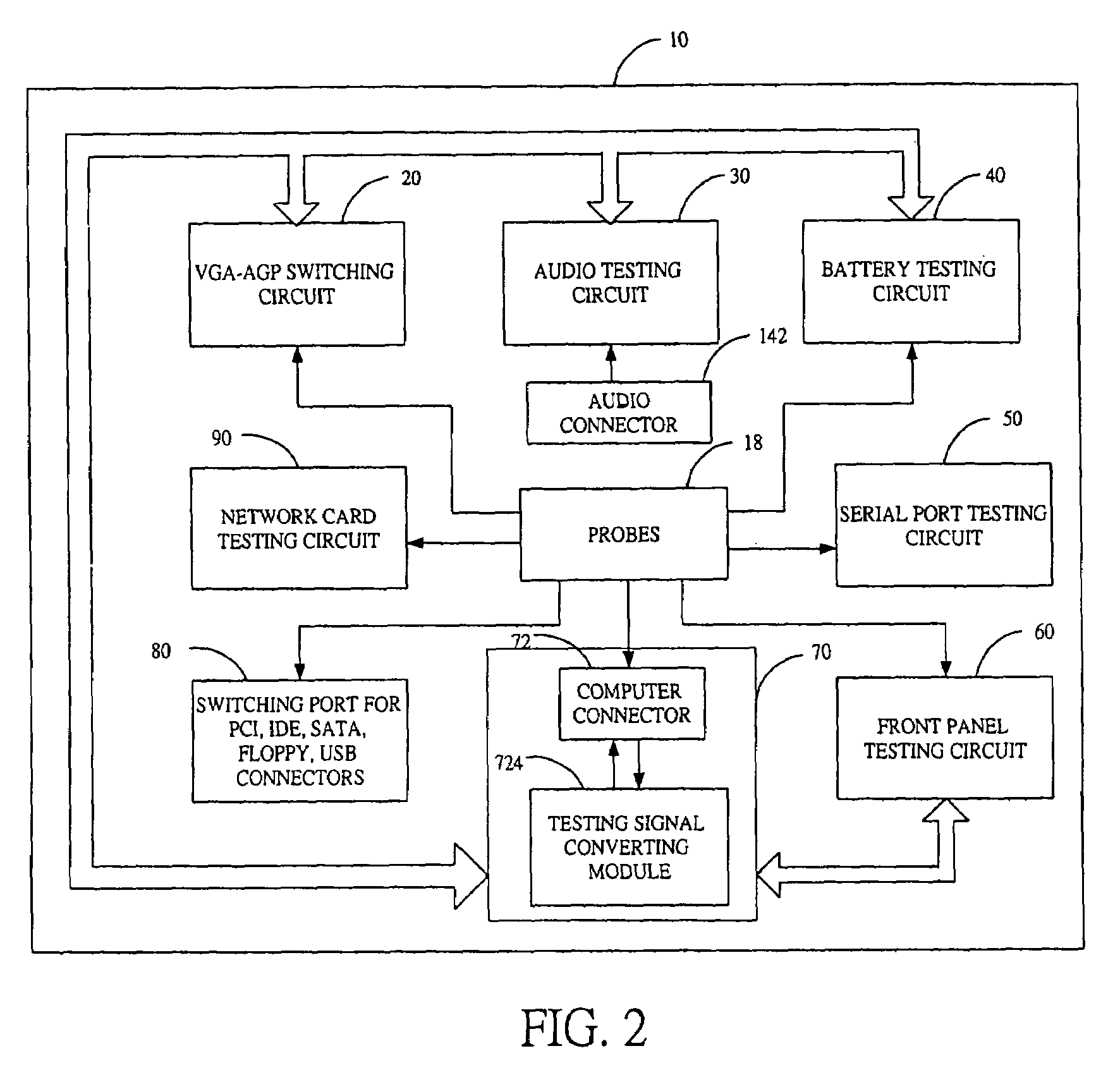
[0020]Referring to FIG. 2, the testing board 10 comprises a VGA-AGP(Video Graphic Array-Accelerated Graphics Port) switching circuit 20, an audio testing circuit 30, a battery testing circuit 40, a serial port testing circuit 50, a fr...


PUM


Abstract

A testing device for testing a printed circuit board comprises a testing signal converting module which comprises a connector for receiving testing signals from the printed circuit board and a converting circuit for converting the testing signals to compatible signals, the converting circuit is coupled to the connector. A testing circuit receives compatible signals from the testing signal converting module.

Description

BACKGROUND OF THE INVENTION[0001]1. Field of the Invention[0002]The present invention relates to a testing device for printed circuit boards, particularly to a testing device for testing overall functions of printed circuit boards.[0003]2. Description of the Related Art[0004]After assembling a printed circuit board, it must have an overall test on the functions to insure the qualities are good. The test mainly aims at the errors that probably occur during the assembling process of the printed circuit board, such as open circuit, short circuit as well as the incorrect connection between the chips. After these detections, the error signals from the testing device are analyzed to find out where the error points are on the circuit board.[0005]In one conventional arrangement, an untested printed circuit board is connected to a testing board with a plurality of terminals by manual work, then outputs the testing signals from the footprints of the chips and slots. Then the testing signals a...

Claims


Application Information

Patent Timeline
Patent Type & Authority Patents(United States)
IPC IPC(8): G01R31/02G01R31/26G01R31/28G06F11/26
CPCG01R31/2815
Inventor PAN, WEN-JUNZHANG, SU-SHUN
Owner HON HAI PRECISION IND CO LTD
Why Eureka
Try Eureka