Programmable self-calibrating vernier and method

a self-calibration and vernier technology, applied in the direction of pulse automatic control, pulse manipulation, pulse technique, etc., can solve the problems of increasing the cost of the test system, the temperature of the substrate is much more difficult to control, and the logic propagation delay is dependent on the power supply voltage and the temperature of the silicon substra

Inactive Publication Date: 2006-04-11
TOP BOX ASSETS L L C
View PDF23 Cites 30 Cited by
  • Summary
  • Abstract
  • Description
  • Claims
  • Application Information

AI Technical Summary

Problems solved by technology

However, as integrated circuit technology has progressed and demanded higher speed, more accurate and more complicated communication equipment, a problem arises to be applied to the timing vernier circuitry is that logic propagation delays are dependent upon the power supply voltage and the temperature of the silicon substrate.
Though the supply voltage sensitivity can be managed to some extent by very tightly regulating the supply voltage, this adds cost to the test system, and also the temperature of the substrate is much more difficult to control.
However, the above technical solution requires continuous monitoring and updating compensation values and also frequent re-calibration of adjustment coefficients to provide accurate timing which is a costly and time consuming operation affecting timing accuracy.

Method used


Image

  • Programmable self-calibrating vernier and method
  • Programmable self-calibrating vernier and method
  • Programmable self-calibrating vernier and method

Examples


Embodiment Construction

[0026]A specialist of ordinary skill in the art will realize that the following description of the present invention is illustrative only and not in any way limiting.

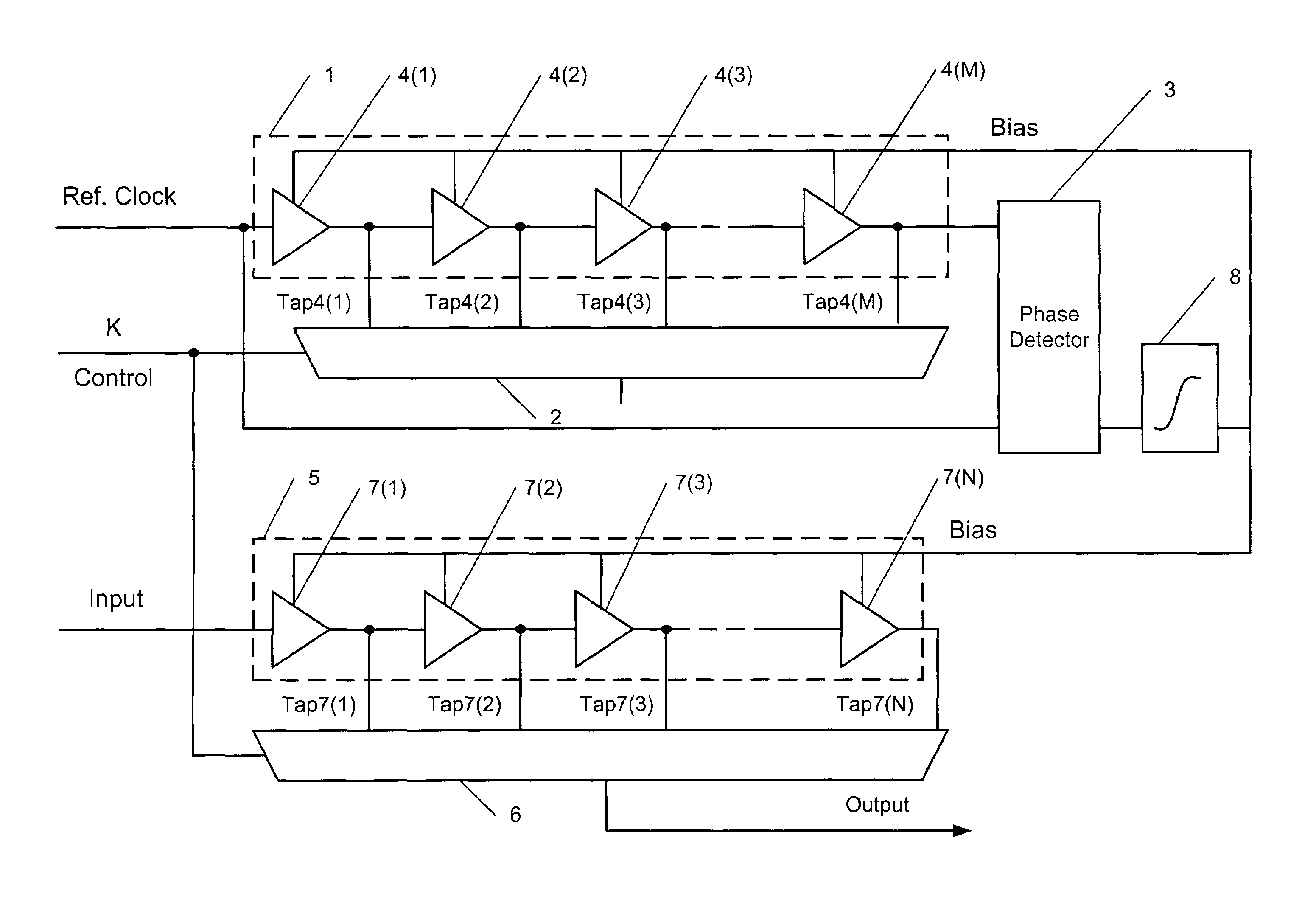
[0027]In FIG. 1 an example block diagram of a self-calibrating programmable vernier using a plurality of delay lines is shown. A chain 5 of delay elements 7(1)–7(N) with a multiplexer 6, which can be implemented as a set of pass-through transistors with appropriate decoder, is used to delay an input signal for a predetermined time interval which is set by control line. The delays may be implemented in, e.g. CMOS buffers with capacitive load. Typical delay circuit topologies are discussed in detail by Mark Horowitz, Chih-Kong Ken Yang and Stefanos Sidiropoulos, in High Speed Electrical Signalling: Overview and Limitations (IV. Synchronization Circuits), Computer Systems Laboratory, Stanford University, Stanford, Calif. 94305, 1998.

[0028]An auxiliary delay circuit 1 is incorporated in the same silicon die to allow the mos...


PUM


Abstract

The present invention relates in general to the field of generation of precise electrical signals, in particular, to a technique for providing accurate delays of signals using a controllable delay line, and is applicable to the areas of high speed communication and memory testing equipment. According to the present invention, an auxiliary reference channel having a delay line which is identical to the main delay line is incorporated into vernier silicon die to allow automatic adjustment of the delay in the main delay line using a reference periodical signal applied to the auxiliary delay line.

Description

[0001]This application claims benefit to Provisional Application No. 60 / 293,053 filed May 21, 2001, the disclosure of which is incorporated herein by reference.BACKGROUND OF THE INVENTION[0002]1. Field of the Invention[0003]The present invention relates in general to the field of generation of precise electrical signals, in particular, to a technique for providing accurate delay of signals using a controllable delay line, and is applicable to the areas of high speed communication and memory testing equipment.[0004]2. Background Art[0005]As the transmission rate of the data communication signals in modern electronic systems continues to increase, new circuitry and methods are needed to accurately clock command data and create precise controllable delays because it is often desired to delay signals at time intervals much shorter than one period of the master oscillator. For example, the master oscillator might have a frequency of 100 MHz. Such an oscillator has a period of 10 nsec. Ho...

Claims


Application Information

Patent Timeline
Patent Type & Authority Patents(United States)
IPC IPC(8): H03L7/06H03K5/00H03K5/13H03K5/135H03L7/07H03L7/081
CPCH03K5/135H03K5/133H03L7/0805H03L7/0812H03L7/07H03K2005/00104H03L7/0816
Inventor ATYUNIN, VASILY GRIGORIEVICHDEAS, ALEXANDER ROGER
Owner TOP BOX ASSETS L L C
Why Eureka
Try Eureka