Semiconductor device to prevent a circuit from being inadvertently active
a level shifting circuit and semiconductor technology, applied in the direction of logic circuit coupling/interface arrangement, pulse generator, pulse technique, etc., can solve the problems of circuit block probably inadvertently activated, unstable output after level shifting, and large transistor siz
- Summary
- Abstract
- Description
- Claims
- Application Information
AI Technical Summary
Problems solved by technology
Method used
Image

Examples
first embodiment
[0042](First Embodiment)
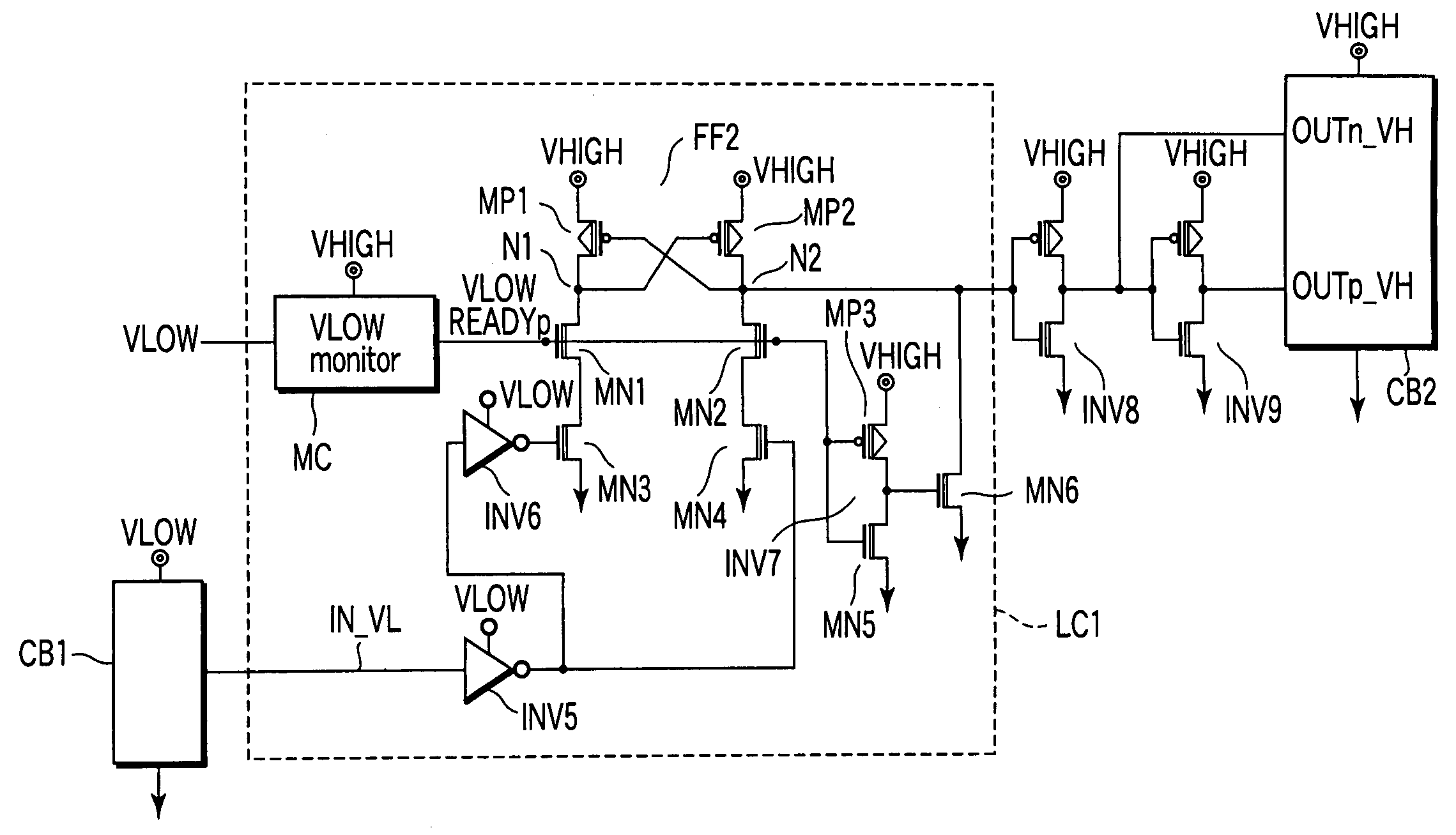
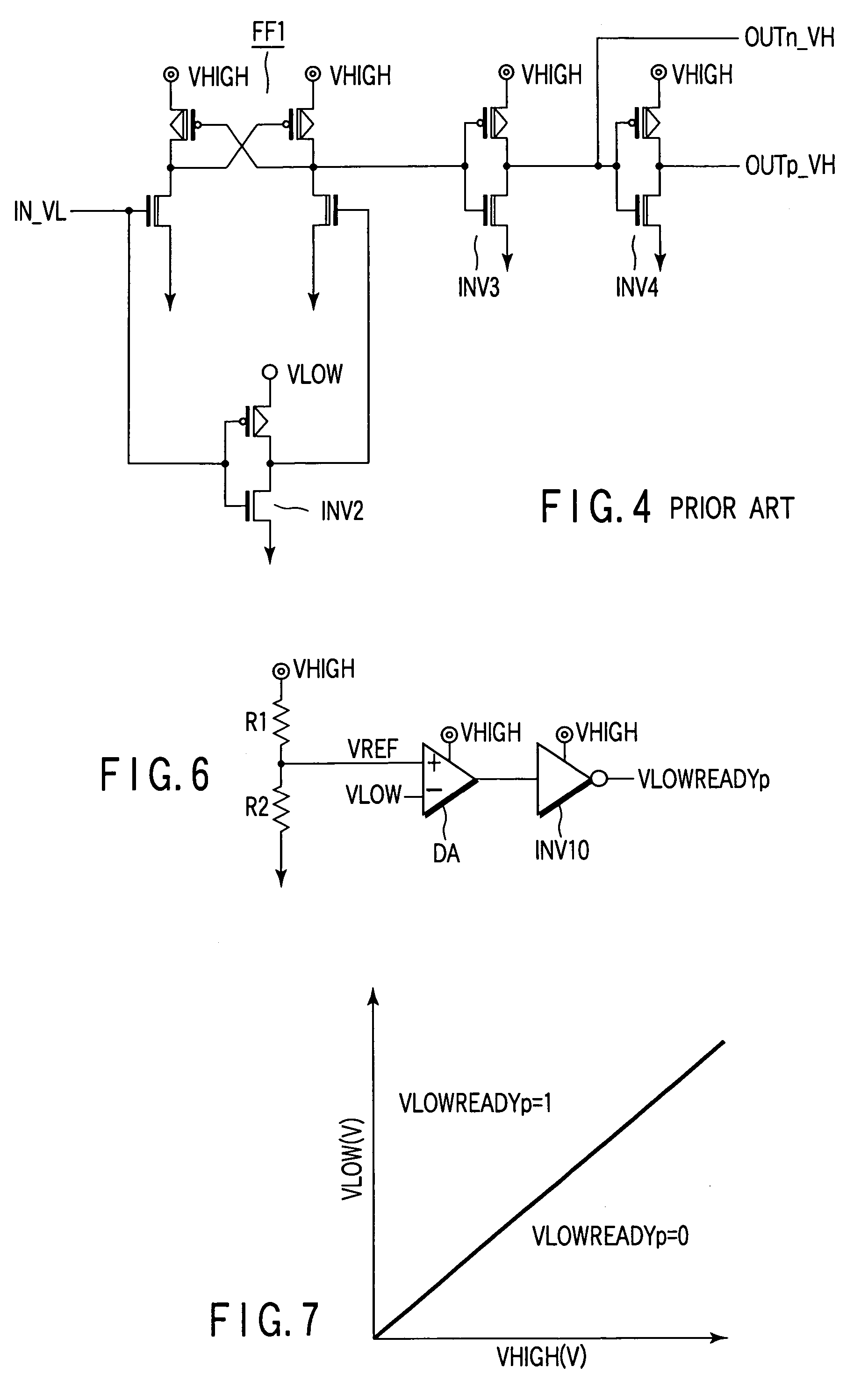
[0043]FIG. 5 is a circuit diagram of a semiconductor device including a level shifting circuit according to a first embodiment of the present invention, FIG. 6 is a circuit diagram of a monitor circuit MC which monitors a first power supply voltage VLOW in FIG. 5, and FIG. 7 is a characteristic diagram showing an output value status of the monitor circuit MC of FIG. 6 in relation to power supply voltages VHIGH / VLOW.
[0044]In FIG. 5, an input signal IN_VL is input into INV5 from a first circuit block CB1. A complementary pair of signals produced from the input signal IN_VL via INV5, INV6 operating on the first power supply voltage VLOW are supplied as input signals of a flip flop FF2 operating on the second power supply voltage VHIGH. The flip flop FF2 comprises cross-coupled PMOS transistors MP1, MP2, and NMOS transistors MN3, MN4 connected to current paths of these transistors in tandem. The complementary pair of signals are input into gates of the NMOS trans...
second embodiment
[0057](Second Embodiment)
[0058]A second embodiment is different from the first embodiment in a generation method of a reference potential VREF of the VLOW monitor circuit MC. In the first embodiment, a voltage between the second power supply voltage VHIGH and ground potential GND is simply divided by resistors R1 and R2. In the second embodiment, as shown in FIG. 8, a VREF node is connected to an anode of a diode DI.
[0059]When the reference voltage VREF simply determined by a resistance ratio is used as in the first embodiment, a voltage range in which the first power supply voltage VLOW is usable is also reduced with an increase of the voltage value of the second power supply voltage VHIGH. For example, when R1=R2, and VLOW<0.5 VHIGH, it is judged that VLOW is low. Therefore, when VHIGH=1.2 V and VLOW=0.6 V or less, or VHIGH=2.0 V and VLOW=1.0 V or less, it is judged that VLOW is low. Therefore, the output of the level shifting circuit is VLOWREADYp=0.
[0060]When the diode DI is dis...
third embodiment
[0062](Third Embodiment)
[0063]FIG. 12 is a circuit diagram of the level shifting circuit according to a third embodiment, and FIG. 13 is a characteristic diagram showing a relation between the output value and the power supply voltages VHIGH / VLOW.
[0064]The third embodiment is different from the first embodiment in that the reference potential generation circuit of VLOW monitor circuit MC is produced by a band gap reference circuit BGR. The band gap reference circuit is capable of obtaining a reference potential having small temperature dependency, and is therefore broadly used. When the reference potential is produced by this circuit, the temperature dependency of VREF in the second embodiment are reduced. When the second power supply voltage VHIGH has a defined value, it can be judged by a determined value whether the first power supply voltage VLOW is high or low. Therefore, the VLOW monitor circuit MC is prevented from narrowing a VLOW operation range.
[0065]A known band gap refer...
PUM
 Abstract
Description
Claims
Application Information
 - R&D Engineer
- R&D Manager
- IP Professional
- Industry Leading Data Capabilities
- Powerful AI technology
- Patent DNA Extraction
Browse by: Latest US Patents, China's latest patents, Technical Efficacy Thesaurus, Application Domain, Technology Topic.
© 2024 PatSnap. All rights reserved.Legal|Privacy policy|Modern Slavery Act Transparency Statement|Sitemap