Supply-state-enabled level shifter interface circuit and method

a level shifter and interface circuit technology, applied in logic circuit coupling/interface arrangement, pulse generator, pulse technique, etc., can solve the problem of resistive degeneration, voltage of node conductor, and create a shoot-through current leakage condition through transistor mnb

Active Publication Date: 2016-02-09
TEXAS INSTR INC
View PDF6 Cites 35 Cited by
  • Summary
  • Abstract
  • Description
  • Claims
  • Application Information

AI Technical Summary

Benefits of technology

[0029]In one embodiment, the invention provides level-shifting circuitry (1-3,1-4) powered by first (VSUPPLY1) and second (VSUPPLY2) supply voltages to avoid shoot-through currents and indeterminate voltage levels and indeterminate logic levels in the level-shifting circuitry (1-3,1-4) during ramping of the first supply voltage (VSUPPLY1), including an input (11) coupled to receive an input enable signal (PGOODIN) that is referenced to a first supply voltage (VSUPPLY1); enable circuit means (1-3) for generating a corresponding level-shifted output enable signal (PGOODOUT) that is referenced to a second supply voltage (VSUPPLY2) in response to the input enable signal (PGOODIN) by operating bias control circuitry (16-1,2,3) so as to prevent shoot-through currents from occurring in the enable circuit means (1-3) during the ramping of the first supply voltage (VSUPPLY1) and also to prevent occurrence of indeterminate voltage levels and indeterminate logic levels of the level-shifted output enable signal (PGOODOUT) during the ramping of the first supply voltage (VSUPPLY1); and enabled level-shifting means (1-4) receiving an input logic signal (VIN) that is referenced to the first supply voltage (VSUPPLY1) for generating a corresponding level-shifted output logic signal (VOUT) that is referenced to the second supply voltage (VSUPPLY2) in response to the input logic signal (VIN) by operating enable circuitry (P1,P2,N1,N2) in response to the level-shifted output enable signal (PGOODOUT) to enable normal level-shifting operation while the first (VSUPPLY1) and second (VSUPPLY2) supply voltages are at normal operating levels and to prevent shoot-through currents from occurring in the enabled level-shifting means (1-4) during the ramping of the first supply voltage (VSUPPLY1) and forcing the level-shifted output logic signal (VOUT) to a predetermined level during the ramping of the first supply voltage (VSUPPLY1).

Problems solved by technology

However, for very low desired shoot-through current levels (of the order of tens of nanoamperes), this forces the resistive degeneration to be so great that level shifting circuit 1-2 may have unacceptable shoot-through current leakage when VSUPPLY1 is at its very low OFF value and the voltage of node ND2 has “floated” up to a sufficiently high level to cause transistor MP1 to be in a weak-inversion ON condition.
One weakness of prior art level-shifting circuit 1-2 is that the voltages of node conductors ND3 and ND4 can “float up” as a result of parasitic capacitive coupling when VSUPPLY1 is low, and this can create a shoot-through current leakage condition through transistor MN2.
This can result in an unacceptably high amount of shoot-through current flowing from VSUPPLY2 to VSS so that the outputs VOUT and VOUTZ are at indeterminate voltage levels and logic states.
The standard prior art cross-coupled P-channel level shifters do not have circuit topologies that avoid the above mentioned shoot-through currents when VSUPPLY1 is OFF and consequently do not have reliable known output logic levels when VSUPPLY1 is OFF.

Method used


Image

  • Supply-state-enabled level shifter interface circuit and method
  • Supply-state-enabled level shifter interface circuit and method
  • Supply-state-enabled level shifter interface circuit and method

Examples


Embodiment Construction

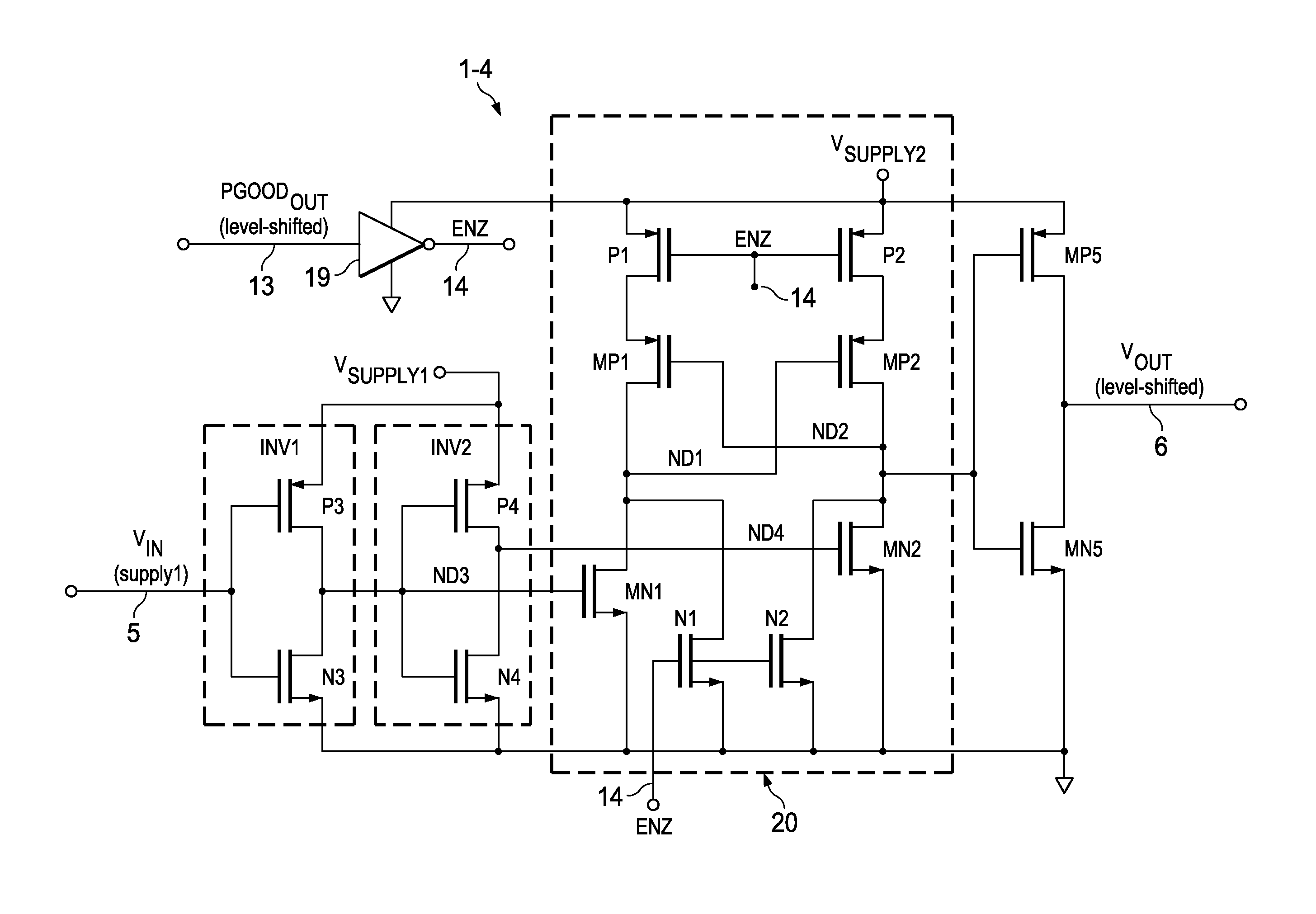
[0034]Referring to FIG. 3, POR (Power On Reset) enable circuit 1-3 receives an input enable signal PGOODIN, which is referenced to a power supply voltage VSUPPLY1. PGOODIN is coupled by conductor 11 to the gate electrodes of a CMOS inverter including a P-channel transistor P7 and a N-channel transistor N7. The source of transistor P7 is connected to VSUPPLY1, and its drain is connected by conductor 12 to the drain of transistor N7, the source of which is connected to ground. PGOODIN also is coupled to the gate electrodes of another CMOS inverter including P-channel transistor P9 and a N-channel transistor N9. The source of transistor P9 is connected to VSUPPLY1, and its drain is connected to the drain of a N-channel intrinsic threshold voltage transistor NA4 having its source connected by a node ND3A to the drain of transistor N9, the source of which is connected to ground. Conductor 12 is also connected to the gate electrode of another inverter including a P-channel transistor P8 a...


PUM


Abstract

An enable circuit receives an input enable signal that is referenced to a first voltage and generates a level-shifted output enable signal referenced to a second voltage. Bias control circuitry prevents shoot-through currents during ramping of the first voltage and from causing indeterminate logic levels of the level-shifted output enable signal. An enabled level-shifting circuit receives an input logic signal that is referenced to the first voltage and generates a level-shifted output logic signal referenced to the second voltage. Enable circuitry operates in response to the level-shifted output enable signal to enable normal level-shifting operation while the first and second voltages are at normal operating levels and prevents shoot-through currents in the enabled level-shifting circuit from causing indeterminate levels of the level-shifted output logic signal.

Description

BACKGROUND OF THE INVENTION[0001]The present invention relates generally to level-shifting circuits having a first power supply voltage level and a different second power supply voltage level and also relates to using techniques that essentially prevent current leakage that causes indeterminate voltage / logic levels during circuit operation when one of the supply voltage levels is at a low level and the other supply voltage level is at a high level. More particularly, the invention relates to level shifting circuitry the operation of which is independent of the order of ramping of the two power supply voltages.[0002]In FIG. 1, conventional level-shifting circuit 1-1 includes a CMOS inverter INV1 having its input coupled to receive an input signal VIN and its output connected by a conductor or node ND3 to the input of another CMOS inverter INV2 and also to the gate of a N-channel transistor MN1 having its source connected to ground. The output of inverter INV2 is connected by a conduc...

Claims


Application Information

Patent Timeline
Patent Type & Authority Patents(United States)
IPC IPC(8): H03K19/185H03K3/356H03K19/0185H03K19/003
CPCH03K3/356104H03K19/018528H03K19/018507H03K3/356182H03K19/00361H03K19/018521
Inventor SHAY, MICHAEL, J.
Owner TEXAS INSTR INC
Why Eureka
Try Eureka