Phase changeable memory devices having multi-level data storage elements and methods of fabricating the same

a memory device and data storage technology, applied in semiconductor devices, semiconductor/solid-state device details, electrical devices, etc., can solve the problems of non-selected cells adjacent to the selected cells being undetected to write, the phase changeable material layer is quite different from the dielectric layer, and the storage data of volatile memory devices

Active Publication Date: 2006-05-02
SAMSUNG ELECTRONICS CO LTD
View PDF7 Cites 68 Cited by
  • Summary
  • Abstract
  • Description
  • Claims
  • Application Information

AI Technical Summary

Problems solved by technology

Volatile memory devices typically lose their stored data when their power supplies are interrupted.
However, the phase changeable material layer is quite different from the dielectric layer

Method used


Image

  • Phase changeable memory devices having multi-level data storage elements and methods of fabricating the same
  • Phase changeable memory devices having multi-level data storage elements and methods of fabricating the same
  • Phase changeable memory devices having multi-level data storage elements and methods of fabricating the same

Examples


Embodiment Construction

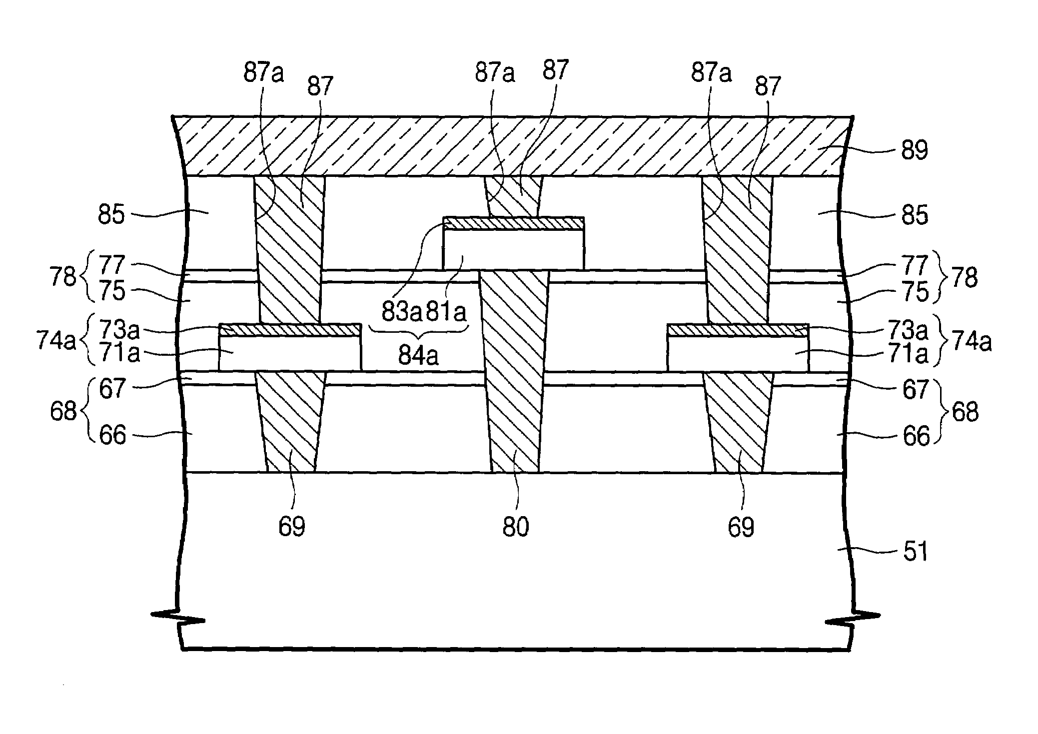
[0032]The present invention now will be described more fully hereinafter with reference to the accompanying drawings, in which typical embodiments of the invention are shown. This invention may, however, be embodied in many different forms and should not be construed as limited to the embodiments set forth herein. Rather, these embodiments are provided so that this disclosure will be thorough and complete, and will fully convey the scope of the invention to those skilled in the art. In the drawings, the relative sizes of regions may be exaggerated for clarity.

[0033]It will be understood that when an element such as a layer, region or substrate is referred to as being “on” another element, it can be directly on the other element or intervening elements may also be present. In contrast, when an element is referred to as being “directly on” another element, there are no intervening elements present.

[0034]FIG. 4 is a top plan view illustrating a portion of a cell array region of a phase...


PUM


Abstract

A phase changeable memory device includes a lower interlayer dielectric layer on a semiconductor substrate. A plurality of first phase changeable data storage elements is disposed on the lower interlayer dielectric layer. A middle interlayer dielectric layer covers the first phase changeable data storage elements and the lower interlayer dielectric layer. A plurality of second phase changeable data storage elements is disposed on the middle interlayer dielectric layer. The first and second phase changeable data storage elements are arrayed in rows and columns such that respective first phase changeable data storage elements are disposed between respective adjacent second phase changeable data storage elements in the rows and columns. A plate electrode overlies the first and second phase changeable data storage elements and is electrically connected to the first and second phase changeable data storage elements. Related fabrication methods are also disclosed.

Description

RELATED APPLICATION[0001]This application claims priority from Korean Patent Application No. 2002-25778 filed on May 10, 2002 in the Korean Intellectual Property Office, the disclosure of which is incorporated herein in its entirety by reference.BACKGROUND OF THE INVENTION[0002]The present invention relates to nonvolatile memory devices and methods of fabricating the same and, more specifically, to phase changeable memory devices and fabrication methods therefor.[0003]Semiconductor memory devices can be classified into volatile memory devices and nonvolatile memory devices. Volatile memory devices typically lose their stored data when their power supplies are interrupted. Nonvolatile (or “less volatile’) memory devices can typically retain their stored data for extended periods of time when their power supplies are interrupted. Accordingly, nonvolatile memory devices are widely used in such devices as memory cards and mobile communications devices.[0004]Nonvolatile memory devices of...

Claims


Application Information

Patent Timeline
IPC IPC(8): H01L21/82H01L27/115H01L27/24
CPCH01L27/2481H01L27/2436H01L45/06H01L45/1233H01L45/144H01L45/126H10B63/84H10B63/30H10N70/231H10N70/8413H10N70/826H10N70/8828H10B69/00
Inventor JOO, JAE-HYUNHORII, HIDEKI
Owner SAMSUNG ELECTRONICS CO LTD
Why Eureka
Try Eureka