Device based on coated nanoporous structure

a nanoporous structure and nanoporous technology, applied in the direction of sustainable manufacturing/processing, final product manufacturing, natural mineral layered products, etc., can solve the problems of difficult material incorporation, limited types of metal oxides which can be formed using sol gel techniques, and inability to form conducting metal materials using sol gel techniques

Inactive Publication Date: 2006-05-16
AERIS CAPITAL SUSTAINABLE IP
View PDF25 Cites 138 Cited by
  • Summary
  • Abstract
  • Description
  • Claims
  • Application Information

AI Technical Summary

Problems solved by technology

The undulating channels make it difficult to incorporate material.
Further, the types of metal oxides which can be formed using sol gel techniques are limited.
In addition, conducting metal materials cannot be formed using sol gel techniques.
Unfortunately, silica is highly insulating and therefore not suitable as a semiconducting or conducting material.
Furthermore, even the pore structure of FIG. 2 is difficult to fill or coat.
Specifically, there is no satisfactory way to uniformly deposit material in both the horizontal pores as well as the vertical pores.

Method used


Image

  • Device based on coated nanoporous structure
  • Device based on coated nanoporous structure
  • Device based on coated nanoporous structure

Examples


Embodiment Construction

[0011]Although the following detailed description contains many specific details for the purposes of illustration, anyone of ordinary skill in the art will appreciate that many variations and alterations to the following details are within the scope of the invention. Accordingly, the embodiments of the invention described below are set forth without any loss of generality to, and without imposing limitations upon, the claimed invention.

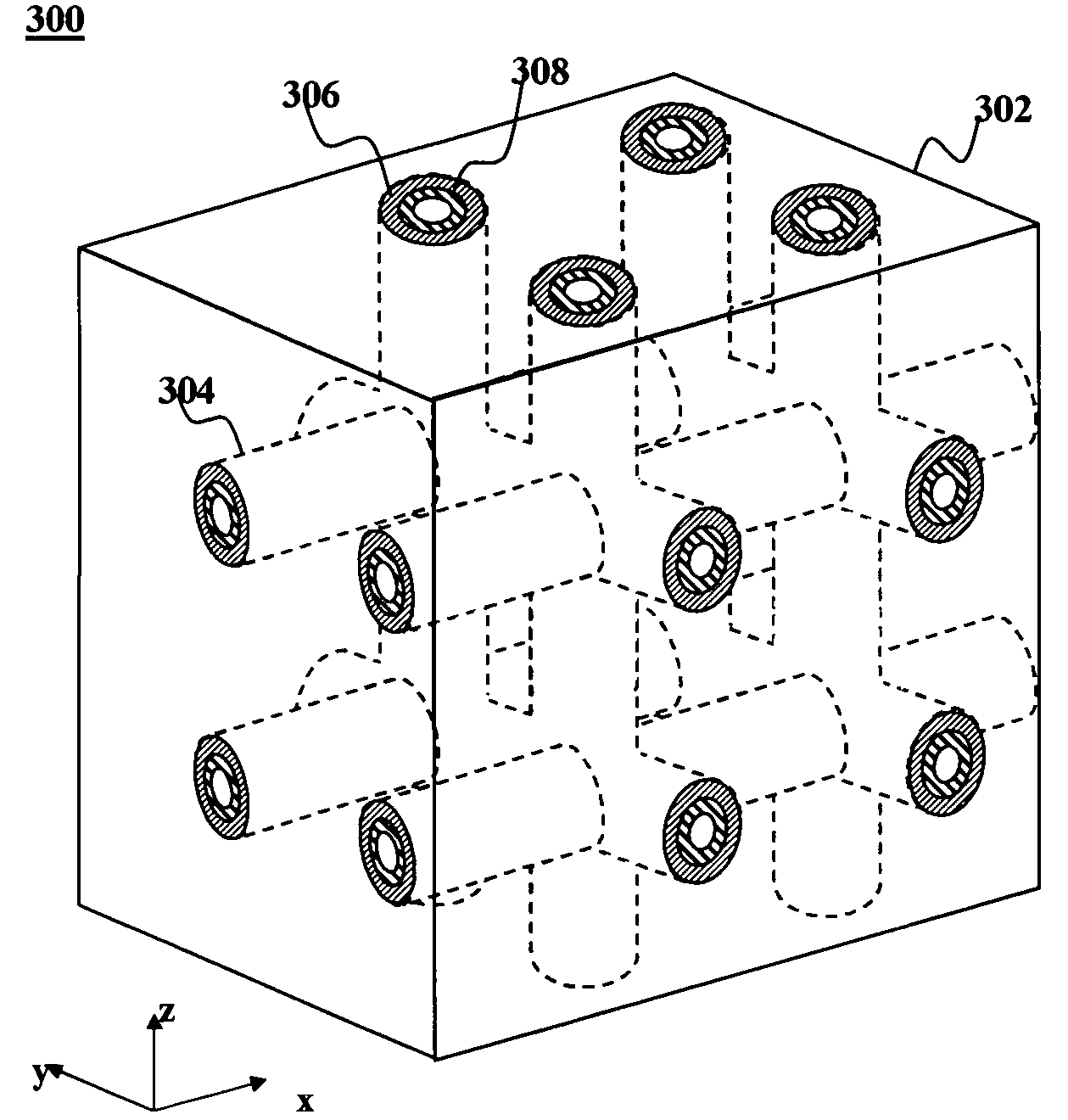
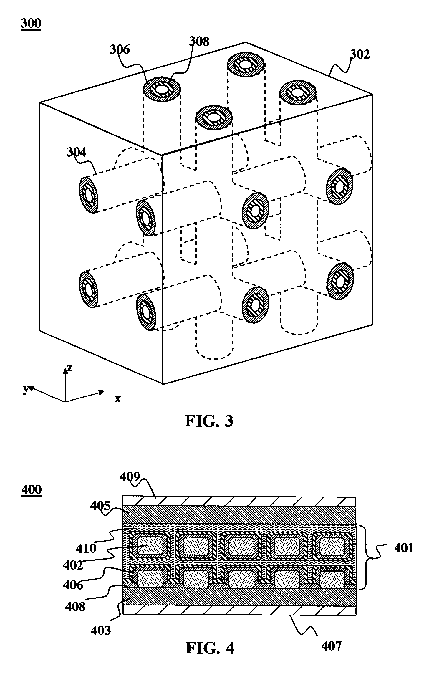
[0012]According to embodiments of the present invention, a device may include an active layer having a mesoporous template having an array of regularly spaced pores. An active material may be deposited on the walls of the pores in a way that conformally coats the walls to a substantially uniform thickness.

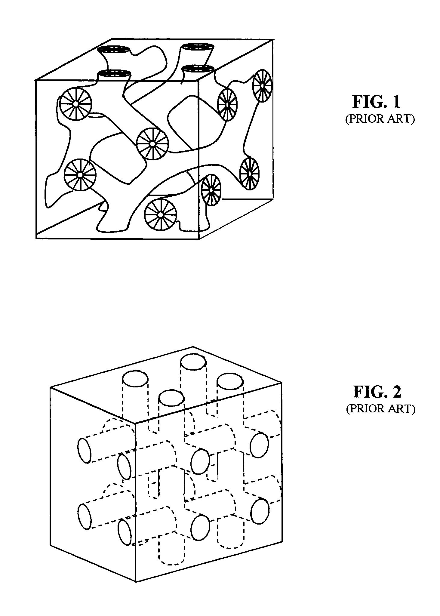
[0013]FIG. 3 depicts an example of a part of a nanostructured apparatus 300 according to an embodiment of the present invention. The apparatus 300 generally includes a mesoporous template 302 having a network of regularly spaced pores 304 (shown in p...


PUM

PropertyMeasurementUnit
pore diameteraaaaaaaaaa
thicknessaaaaaaaaaa

Abstract

A nanostructured apparatus may include a mesoporous template having an array of regularly-spaced pores. One or more layers of material may conformally coat the walls to a substantially uniform thickness. Such an apparatus can be used in a variety of devices including optoelectronic devices, e.g., light emitting devices (such as LEDs, and lasers) and photovoltaic devices (such as solar cells) optical devices (luminescent, electro-optic, and magnetooptic waveguides, optical filters, optical switches, amplifies, laser diodes, multiplexers, optical couplers, and the like), sensors, chemical devices (such as catalysts) and mechanical devices (such as filters for filtering gases or liquids).

Description

FIELD OF THE INVENTION[0001]This invention is directed to photovoltaic devices and more particularly to nanostructured photovoltaic devices and methods for manufacture of nanostructured photovoltaic devices.BACKGROUND OF THE INVENTION[0002]Many devices could benefit from an active layer having a network of regularly interconnected nanometer scale pores, including optoelectronic devices (e.g. photovoltaic cells, organic LEDs, and lasers), optical devices (e.g. waveguides and optical filters), mechanical devices (e.g. filters and separation media), and chemically-active devices (e.g. catalysts. In each of these and other device applications, it would be beneficial to have a nanometer-scale network comprised of either semiconducting (e.g. semiconducting metal oxides), conducting materials (e.g. metals), and / or sequentially placed conformal layers of semiconducting and conducting materials as a component of such devices.[0003]Recently, mesoporous templates have been fabricated using sol...

Claims


Application Information

Patent Timeline
Patent Type & Authority Patents(United States)
IPC IPC(8): B32B3/26H01L31/00
CPCB82Y10/00H01L27/301H01L31/035281H01L51/4213H01L51/5012H01L51/0036H01L51/0038Y02E10/549H01L51/0055H01L51/0078H01L51/4253H01L51/0046Y10T428/249957Y10T428/24999Y10T428/24996Y10T428/249987Y10T428/249969Y10T428/249981Y10T428/249975Y10T428/249979Y10T428/249953Y02P70/50H10K39/10H10K85/114H10K85/113H10K85/211H10K85/623H10K85/311H10K30/10H10K30/30H10K50/11
Inventor SAGER, BRIAN M.
Owner AERIS CAPITAL SUSTAINABLE IP
Why Eureka
Try Eureka