Reuse in semiconductor measurement recipes

a semiconductor and recipe technology, applied in the field of parameter reuse techniques, can solve the problems of reducing device yield, increasing device density and complexity, and affecting the reliability of recipe, so as to improve the reliability and tool performance

Inactive Publication Date: 2006-05-16
KLA TENCOR TECH CORP
View PDF2 Cites 25 Cited by
  • Summary
  • Abstract
  • Description
  • Claims
  • Application Information

AI Technical Summary

Benefits of technology

[0009]Componentization of the recipe into reusable sub-recipes will enable at least selected reuse of previously collected groupings of recipe parameters based on dependency analysis, which in turn reduces the recipe creation time and often avoids the repeated use of a physical tool and physical wafers which all reduces labor and tool usage costs.
[0011]Use and consultation of recipe parameter dependencies proposed by this method can lead a measurement setup engineer to reuse more appropriate groups of parameters and avoid use of inappropriate recipe parameters which will may cause the recipe to fail or perform poorly. This reduces the need for setup engineer training and improves recipe reliability and tool performance over known semiconductor measurement recipe techniques.

Problems solved by technology

Generally, the industry of semiconductor manufacturing involves highly complex techniques for integrating circuits into semiconductor materials.
Due to the large number of processing steps and the decreasing size of semiconductor devices, the semiconductor manufacturing process is prone to processing defects that decrease device yields.
However, as semiconductor devices increase in density and complexity, semiconductor measurement has likewise become more complex.
This is repetitive redundant work costly in manpower and tool costs and it allows more opportunity for human and tool errors during all the setup processes.
The result is often costly, unreliable, poor performing tool recipes.

Method used


Image

  • Reuse in semiconductor measurement recipes
  • Reuse in semiconductor measurement recipes
  • Reuse in semiconductor measurement recipes

Examples


Embodiment Construction

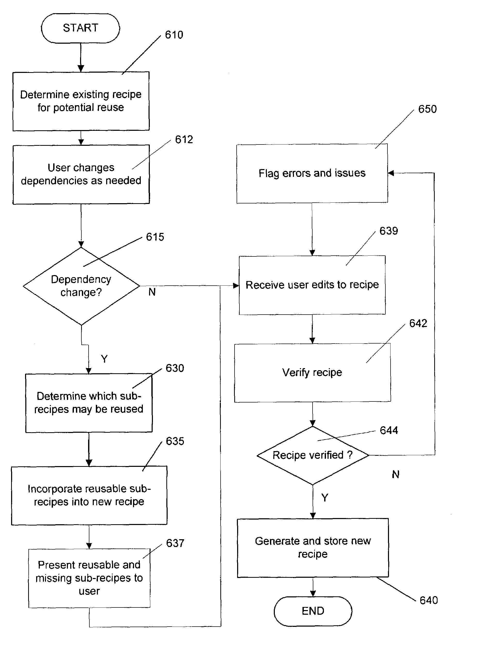
[0019]Dependency-based sub-recipe reuse consistent with the present invention is intended to reduce the cost and improve the reliability and performance of setting up semiconductor measurement recipes. It works for all semiconductor devices to be measured, all layers of the process used to make the device, all possible measurement tools, and all goals semiconductor fabrication facilities may have in measuring these semiconductor devices in isolation or disposed within a wafer.

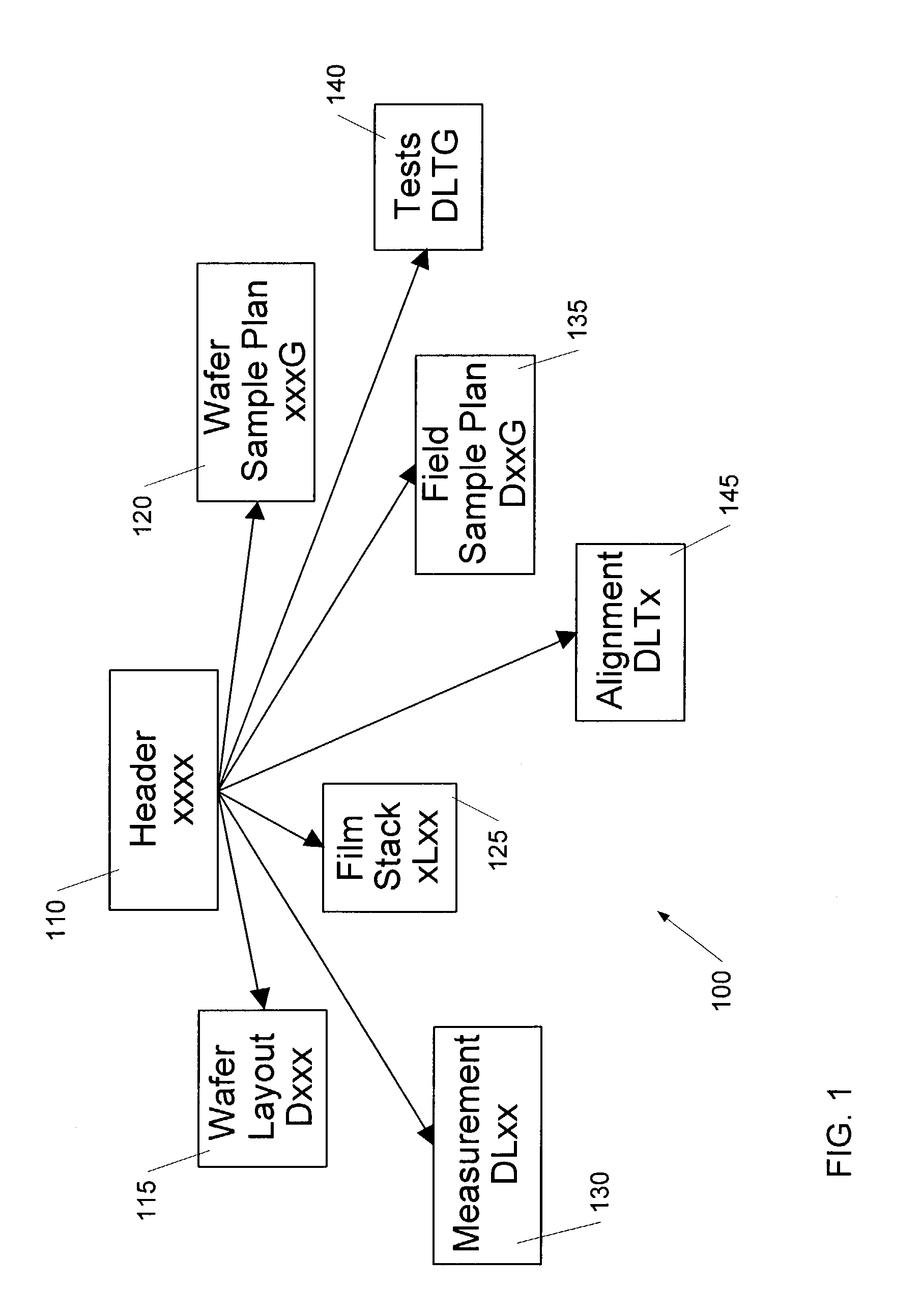
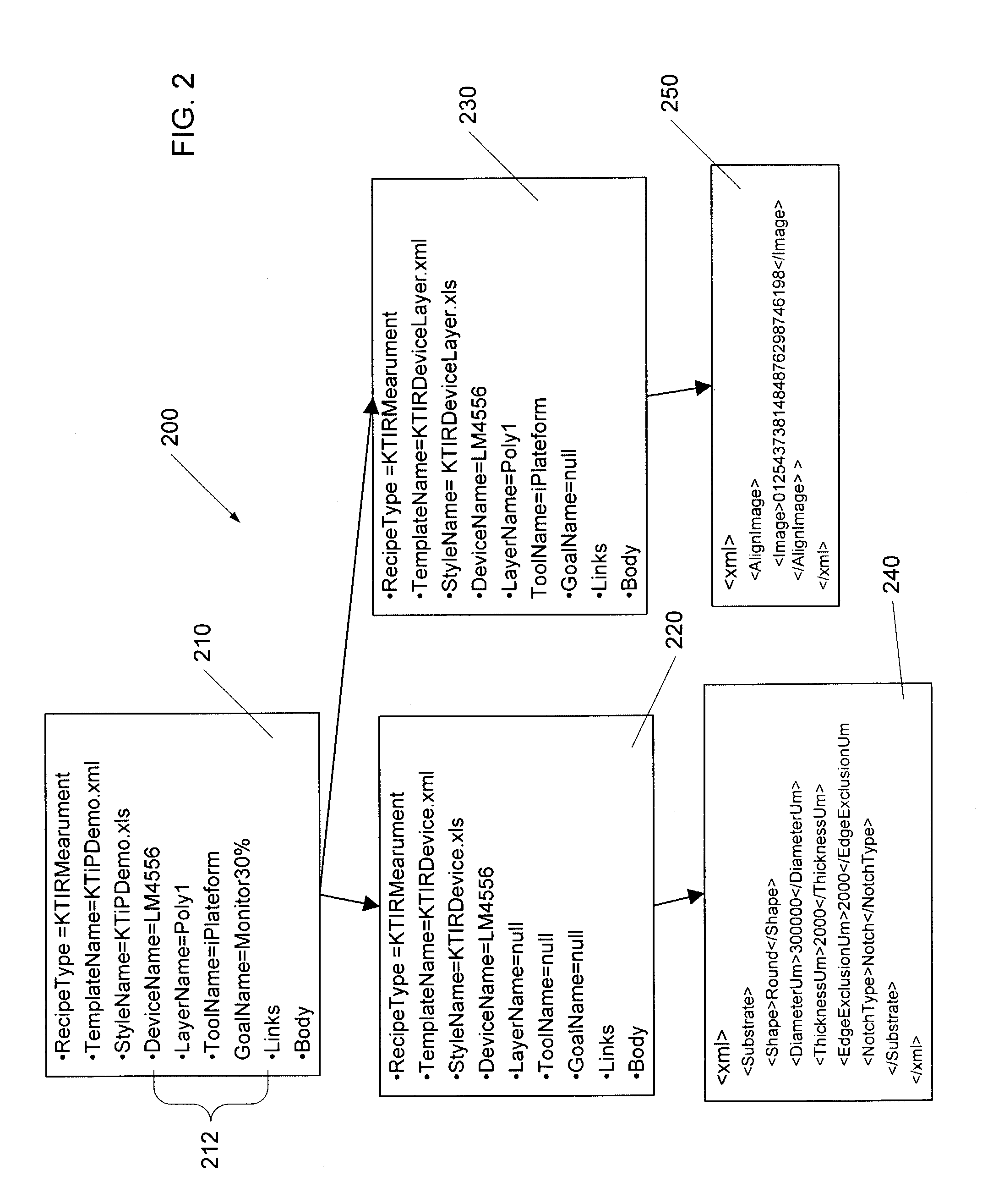
[0020]In accordance with a disclosed embodiment of the invention, the parameter dependencies that are believed conveniently intuitive to semiconductor measurement tool users and activities include the Device, Layer, Tool, and Goal dependencies, the set of which will be referred to DLTG. The Device dependency describes the particular semiconductor circuit or product upon which measurement is desired and how it is geographically laid out on the wafer. Though certainly not meant to be limiting in any way, example ...


PUM


Abstract

A semiconductor measurement recipe architecture organized to include reusable sub-recipes, each defining at least one parameter associated with either a semiconductor wafer and / or a semiconductor disposed thereon, is disclosed. This recipe architecture will include a set of parameter dependencies, one or more which having a respective relationship with of the sub-recipes to permit safe and reliable sub-recipe reuse. Also disclosed is a recipe generation method including: determining an appropriate baseline existing recipe that's organized to include a set of parameter dependencies and dependency related sub-recipes; perceiving a dependency change; determining which, if any, of the sub-recipes of the existing recipe remain unaffected after the dependency change(s); and generating a new recipe using at least one of the sub-recipes found to be unaffected.

Description

RELATED APPLICATIONS[0001]This application claims priority benefit under 35 U.S.C. § 119(e)(1) to U.S. Provisional Application No. 60 / 399,500 filed Jul. 29, 2002, which is incorporated herein fully by reference.TECHNICAL FIELD[0002]The present invention is generally directed to parameter reuse techniques, and is particularly concerned with selective reuse of one or more components of a parameter recipe for use in semiconductor measurement and verification activities involving semiconductor wafers and semiconductors disposed thereon.BACKGROUND[0003]Generally, the industry of semiconductor manufacturing involves highly complex techniques for integrating circuits into semiconductor materials. Due to the large number of processing steps and the decreasing size of semiconductor devices, the semiconductor manufacturing process is prone to processing defects that decrease device yields. Testing procedures to eliminate these processing defects from the processing steps are therefore critica...

Claims


Application Information

Patent Timeline
Patent Type & Authority Patents(United States)
IPC IPC(8): G06F19/00
CPCG05B19/41875G05B2219/45031G05B2219/32142Y02P90/02
Inventor YOUNG, SCOTTDAVID, DOMINIC GERALD
Owner KLA TENCOR TECH CORP
Why Eureka
Try Eureka