Sheet beam-type testing apparatus

a beam-type testing and beam-type technology, applied in the direction of photomechanical treatment originals, material analysis using wave/particle radiation, instruments, etc., can solve the problems of affecting the degree of vacuum of the beam-type defect testing apparatus, the inability to accurately measure the defect, etc., to achieve stable vacuum degree, stabilize the processing of the sample, and minimize the influence of the degree of vacuum

Inactive Publication Date: 2006-05-23
EBARA CORP
View PDF60 Cites 52 Cited by
  • Summary
  • Abstract
  • Description
  • Claims
  • Application Information

AI Technical Summary

Benefits of technology

[0023]a mini-environment device for supplying a clean gas to the object under testing to prevent dust from attaching to the object under testing;
[0120]In the twelfth embodiment, electron irradiating means is further provided for irradiating a primary electron beam to each of a plurality of regions under testing to emit secondary electron beams from the sample, wherein the image capturing means detects the secondary electron beams emitted from the plurality of regions under testing, thereby making it possible to sequentially capture the images of the plurality of regions under testing.

Problems solved by technology

However, the electron beam-type defect testing apparatus also has a disadvantage in that it is inferior to the optical one in the throughput.
However, it takes so long testing time that it is expected to develop a defect testing apparatus which can rapidly conduct a test.
Generally, a testing apparatus is expensive and low in throughput as compared with other process apparatuses, so that it is presently used after critical steps, such as after etching, deposition, CMP (chemical-mechanical polishing) planarization processing, and so on.

Method used


Image

  • Sheet beam-type testing apparatus
  • Sheet beam-type testing apparatus
  • Sheet beam-type testing apparatus

Examples


first embodiment

EMBODIMENT RELATING TO OVERALL STRUCTURE OF APPARATUS (FIRST EMBODIMENT)

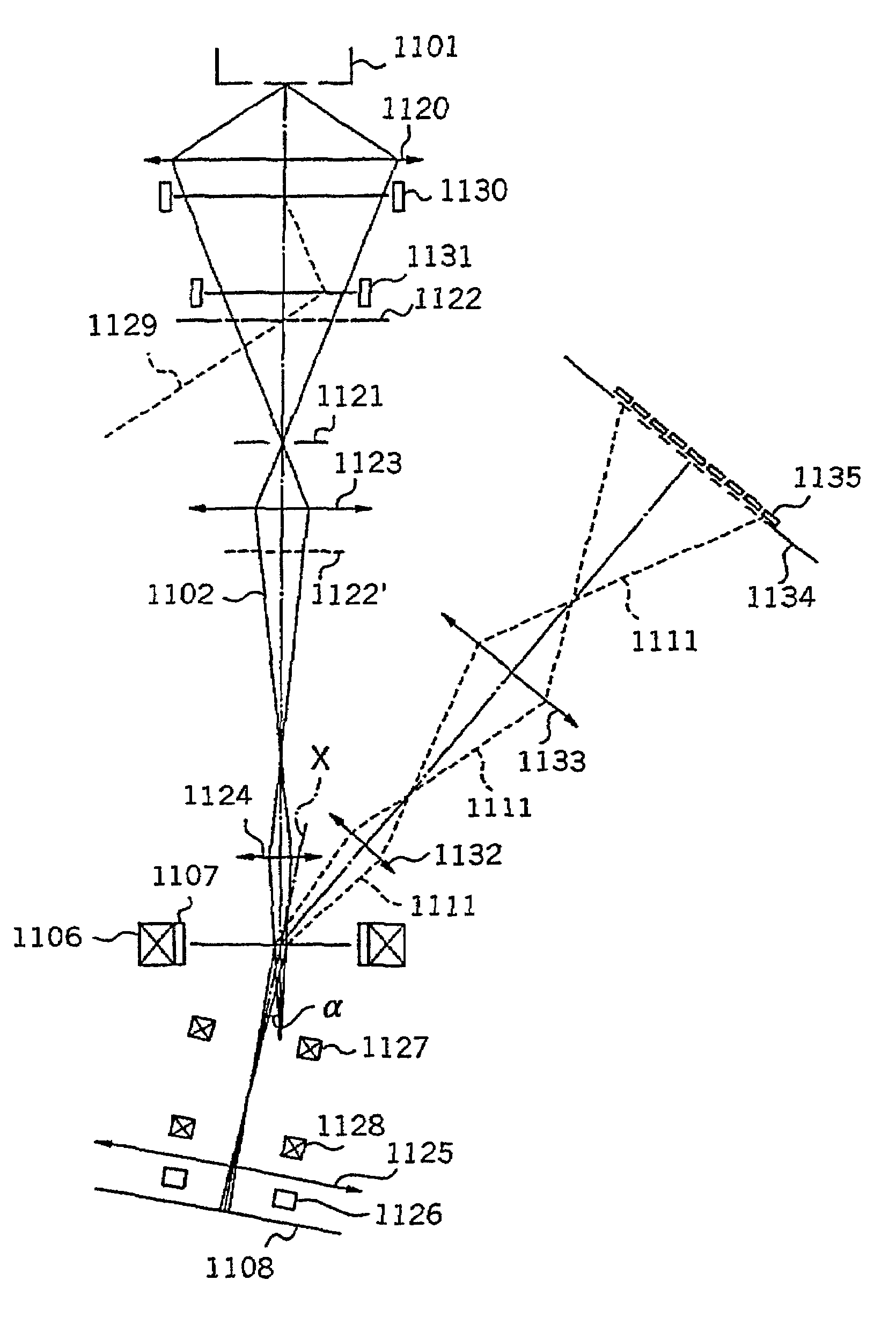
[0180]A first embodiment of the charged particle beam apparatus according to the present invention relates to an electron beam-type image projection system, so that the image projection system will be described first.

[0181]The image projection system involves collectively irradiating a region under observation on a sample with a primary electron beam, i.e., irradiating a fixed area without scanning, and focusing a secondary electron beam from the irradiated region collectively on a detector (a combination of a micro-channel plate and a fluorescent plate) through a lens system as an image of the secondary electron beam. This image is transduced into an electric signal by a two-dimensional CCD (solid-state imager device) or TDI-CCD (line image sensor) to output on a CRT or to store in a storage device. From this image information, defects on the sample wafer (a semiconductor (Si) wafer in the middle of a process) ...

second embodiment

EMBODIMENT RELATING TO TESTING APPARATUS (SECOND EMBODIMENT)

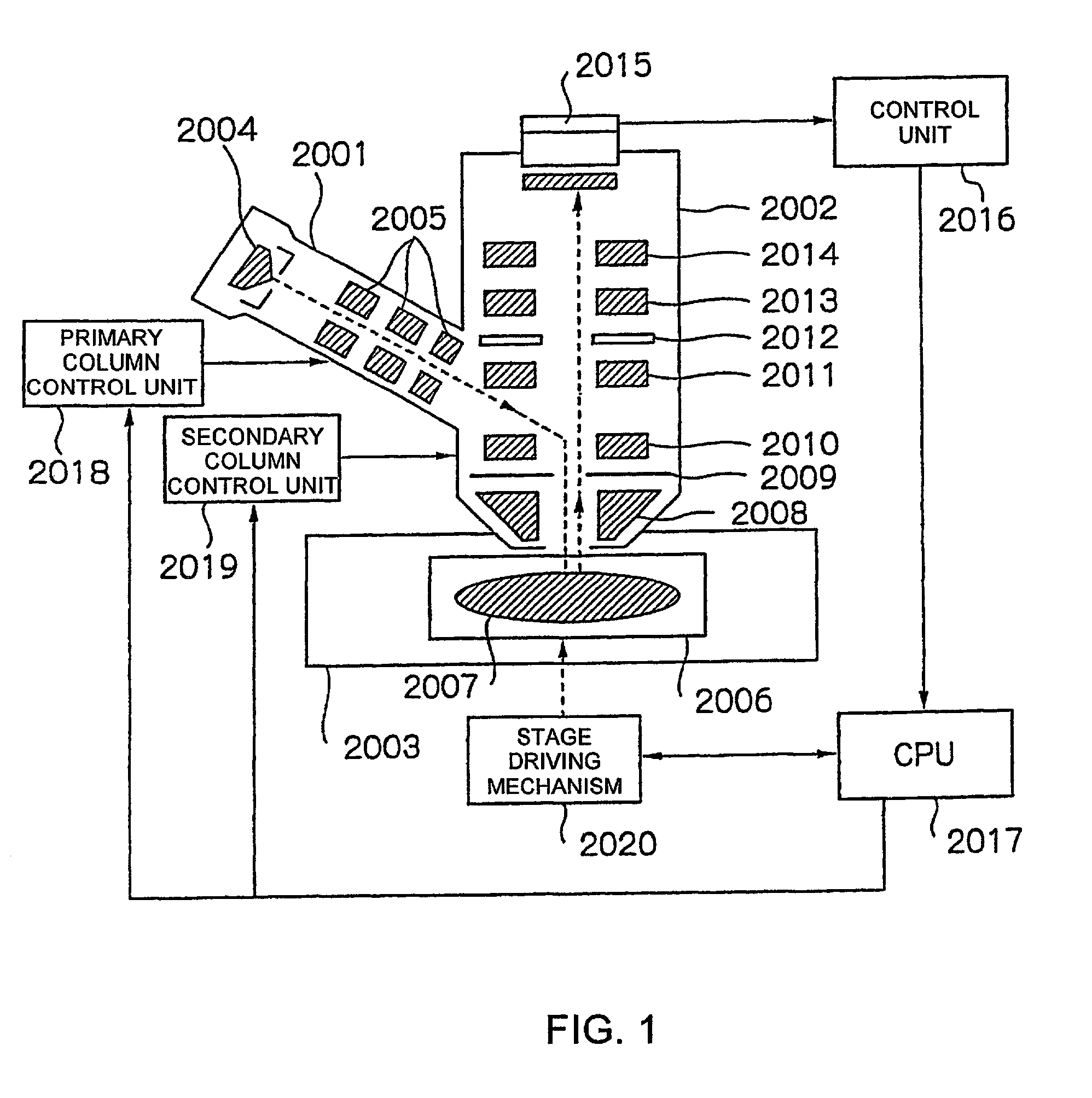
[0240]The second embodiment of the present invention relates to an electron beam apparatus suitable for testing, using an electron beam, defects in patterns formed on the surface of an object under testing, and more particularly, to an electron beam apparatus suitable for a testing apparatus useful, for example, in detecting defects on a wafer in a semiconductor manufacturing process, which includes irradiating an object under testing with an electron beam, capturing secondary electrons which vary in accordance with the properties of the surface thereof to form image data, and testing patterns formed on the surface of the object under testing based on the image data at a high throughput, and a method of manufacturing devices at a high yield rate using such an electron beam apparatus.

[0241]As an apparatus for testing defects of a wafer using an electron beam, an apparatus using a scanning electron microscope (SEM) already co...

third embodiment

EMBODIMENT RELATING TO COLUMN (THIRD EMBODIMENT)

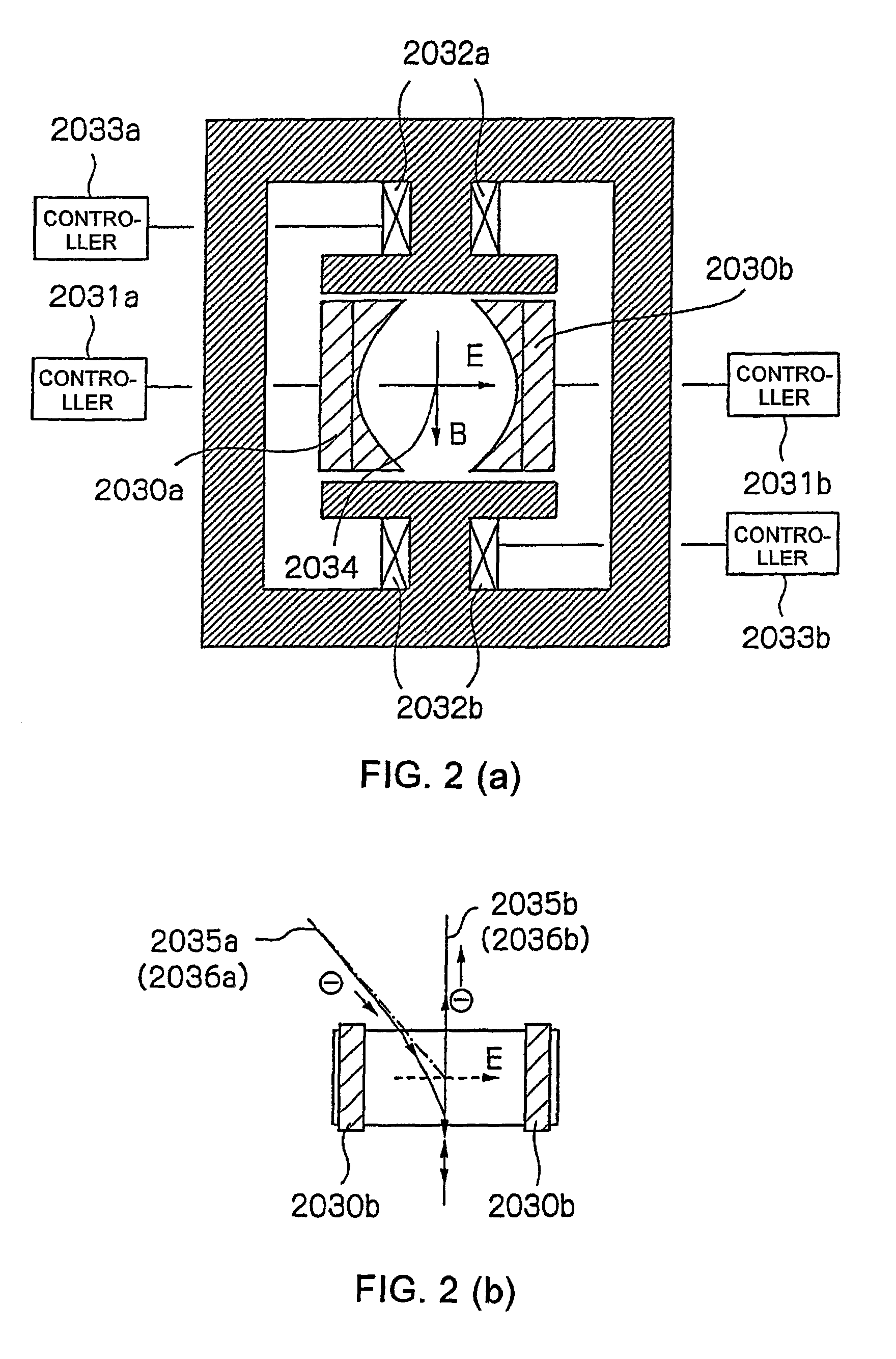
[0324]Now, an electron beam apparatus, which is a third embodiment of the electron beam apparatus according to the present invention, will be described with reference to FIG. 15. This electron beam apparatus is suitable for evaluating and testing samples such as wafers, masks and so on which have patterns with a minimum line width of 0.1 micron or less at a high throughput and high reliability, and can be used for manufacturing of devices.

[0325]An electron beam apparatus using multi-beams is already known. For example, a known electron beam apparatus emits one or more electron beams converged to a predetermined diameter from an electron beam source which is focused on the surface of a sample under testing, moves the sample under testing to scan the electron beams on the surface of the sample under testing, detects secondary electron beams emitted from the sample under testing and reflected electron beams using a plurality of detecting ...


PUM

PropertyMeasurementUnit
widthaaaaaaaaaa
diameteraaaaaaaaaa
work functionaaaaaaaaaa

Abstract

An electron beam apparatus such as a sheet beam based testing apparatus has an electron-optical system for irradiating an object under testing with a primary electron beam from an electron beam source, and projecting an image of a secondary electron beam emitted by the irradiation of the primary electron beam, and a detector for detecting the secondary electron beam image projected by the electron-optical system. Specifically, the electron beam apparatus comprises beam generating means 2004 for irradiating an electron beam having a particular width, a primary electron-optical system 2001 for leading the beam to reach the surface of a substrate 2006 under testing, a secondary electron-optical system 2002 for trapping secondary electrons generated from the substrate 2006 and introducing them into an image processing system 2015, a stage 2003 for transportably holding the substrate 2006 with a continuous degree of freedom equal to at least one, a testing chamber for the substrate 2006, a substrate transport mechanism for transporting the substrate 2006 into and out of the testing chamber, an image processing analyzer 2015 for detecting defects on the substrate 2006, a vibration isolating mechanism for the testing chamber, a vacuum system for holding the testing chamber at a vacuum, and a control system 2017 for displaying or storing positions of defects on the substrate 2006.

Description

FIELD OF THE INVENTION[0001]In semiconductor processes, design rules are now going to enter the era of 100 nm, and the production scheme is shifting from small-kind mass production represented by DRAM to a multi-kind small production such as SOC (silicon on chip). Associated with this shifting, the number of manufacturing steps has been increased, and an improved yield of each process is essential, so that testing for defects caused by the process becomes important. The present invention relates to a charged particle beam suitable for a sheet beam-type testing apparatus for testing a wafer after each of steps in a semiconductor process, and more particularly, to a sheet beam-type testing apparatus using a charged particle beam such as an electron beam, and a semiconductor device manufacturing method and an exposure method using the testing apparatus.BACKGROUND ART[0002]With the trend of increasingly higher integration of semiconductor devices and finer patterns, a need exists for hi...

Claims


Application Information

Patent Timeline
Patent Type & Authority Patents(United States)
IPC IPC(8): H01J37/28G01N23/225G03F1/76G03F1/78H01J37/06H01J37/073H01J37/18H01J37/20H01J37/22H01J37/244
CPCG01N23/225H01J37/073H01J37/185H01J37/20H01J37/222H01J37/244H01J37/28H01J37/06H01J2237/2817H01J2237/082H01J2237/202H01J2237/20228H01J2237/204H01J2237/22H01J2237/24564H01J2237/2806H01J2237/2816H01J37/29
Inventor NAKASUJI, MAMORUNOJI, NOBUHARUSATAKE, TOHRUKIMBA, TOSHIFUMISOBUKAWA, HIROSIKARIMATA, TSUTOMUOOWADA, SHINYOSHIKAWA, SHOJISAITO, MUTSUMI
Owner EBARA CORP
Why Eureka
Try Eureka