Cold clock power reduction

a clock power and cold technology, applied in the field of latch timing circuits, can solve the problem of more clock power than desired, and achieve the effect of reducing clock power and clock power consumption

Inactive Publication Date: 2006-05-23
FUJITSU LTD
View PDF18 Cites 8 Cited by
  • Summary
  • Abstract
  • Description
  • Claims
  • Application Information

AI Technical Summary

Benefits of technology

[0008]A multimode latch timing circuit is disclosed having at least two modes of operation. The latch timing circuit has two sets of timing latches for controlling the flow of data in a logical path. In one mode of operation, the latch timing circuit operates as a two-phase transparent latch timing circuit with the first set of latches being driven by a first phase clock signal and the second set of latches being driven by a second phase clock signal. In a reduced clock power mode of operation, the first set of latches may be held in a transparent state with a constant bias voltage, reducing clock power consumption by up to half. In long paths, the first set of latches may be held in a transparent state with the second set of latches driven by the second phase clock signal. In short paths, the first set of latches may be held in a transparent state with the second set of latches driven by a second phase clock signal comprising short duty cycle pulses with a pulse width selected to prevent a race condition. The first mode of operation may be used during testing and bring up of an integrated circuit incorporating the latch timing circuit. If the timing delays of the integrated circuit permit operation in the reduced clock power mode of operation, the integrated circuit may be programmed to operate in the reduced clock power mode in one or more logical paths.

Problems solved by technology

A drawback of the conventional two-phase latch timing circuit 100 is that it consumes more clock power than desired.

Method used


Image

  • Cold clock power reduction
  • Cold clock power reduction
  • Cold clock power reduction

Examples


Embodiment Construction

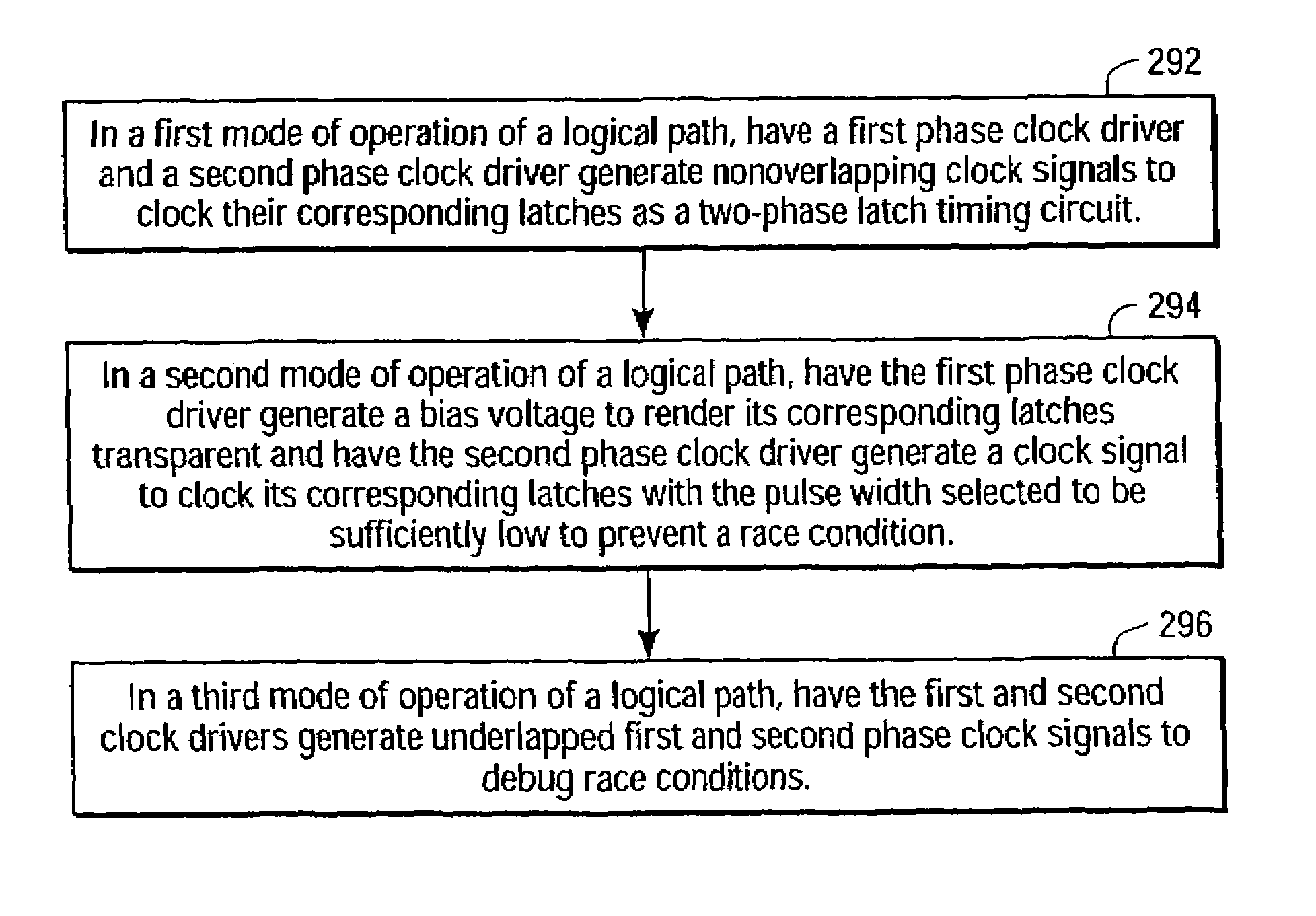
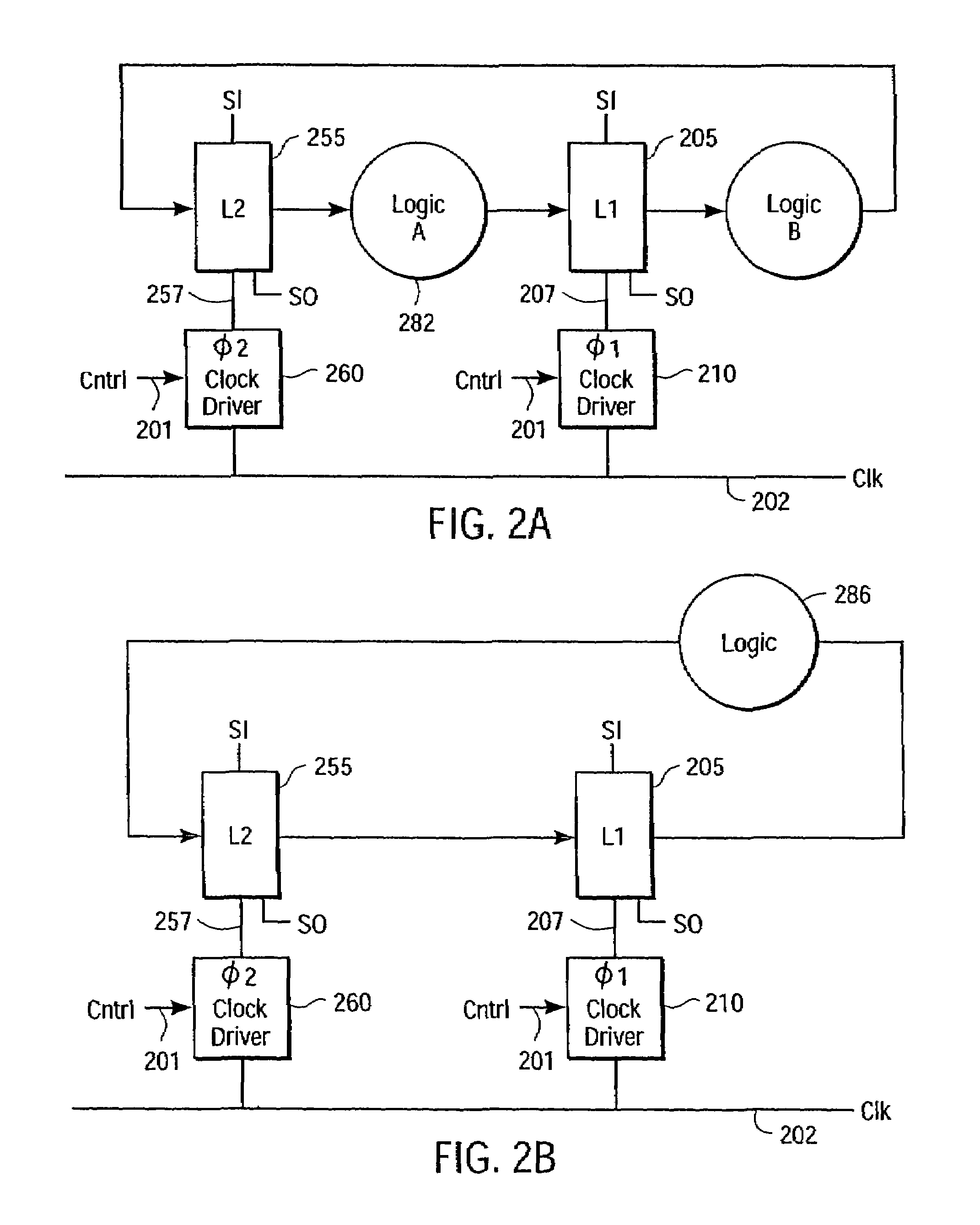
[0026]The present invention generally comprises a multi-mode latch timing circuit and method that permits a single latch timing circuit to be used in an least two different modes of operation. FIGS. 2A–2C are block diagrams showing latch timing circuits in accord with one embodiment of the present invention. FIG. 2D is a flow chart showing illustrative modes of operation. One mode of operation 292 is as a conventional two-phase latch timing circuit having two non-overlapping latch states of a first and a second set of latches. Another mode of operation 294 holds the first set of latches in a transparent state to reduce clock power consumption. Additionally, in one embodiment, in a third mode of operation 296 the two phase clocking signals may be altered from a conventional overlap mode to an underlap mode, which is beneficial to debug race conditions.

[0027]Referring to FIG. 2A, a first set of latches 205 (e.g., at least one “L1” latch”) is part of a data path with a second set of la...


PUM


Abstract

A multi-mode latch timing circuit has a first set of latches and a second set of latches in each logical path. In a first mode of operation, first and second phase clock signals are provided so that the latch timing circuit functions as a two-phase non-overlapping transparent latch timing circuit. In a second mode of operation, the first set of latches is held in a transparent state in some or all of the logical paths, thereby reducing clock power. In one embodiment, the first set of latches in each long path is held in a transparent state while the second phase clock signal is supplied to the second set of latches. In one embodiment, the first set of latches in each short path is held in a transparent state while a second phase clock signal comprised of shortened duty cycle pulses is supplied to the second set of latches.

Description

RELATED APPLICATIONS[0001]This application is a divisional of U.S. patent application Ser. No. 10 / 040,577, by Robert Masleid, which was filed on Dec. 28, 2001 now U.S. Pat. No. 6,668,357 and claims priority under 35 U.S.C.§ 119(e) to U.S. patent application Ser. No.: 60 / 301,890, “Cold Clock Power Reduction,” by Robert Masleid, which was filed Jun. 29, 2001, the entire contents of which are hereby incorporated by reference in the present patent application.BACKGROUND OF THE INVENTION[0002]1. Field of the Invention[0003]The present invention is generally related to latch timing circuits for integrated circuits.[0004]2. Description of Background Art[0005]Transparent latch timing circuits are commonly used in integrated circuits to regulate the flow of logical data signals in each logical path. Referring to FIG. 1, a common latch timing design is a two-phase non-overlapping latch timing circuit 100. During a first portion of the clock cycle, the L1 latch(es) are transparent, allowing a ...

Claims


Application Information

Patent Timeline
Patent Type & Authority Patents(United States)
IPC IPC(8): G06F17/50G06F1/04G06F1/12G06F1/32H03K3/012H03K3/037H03K5/135H03K19/173
CPCG06F1/04G06F1/3203G06F1/3237H03K5/135G06F1/324Y02B60/1221H03K3/012Y02B60/1217Y02D10/00
Inventor MASLEID, ROBERT P
Owner FUJITSU LTD
Why Eureka
Try Eureka