
Image display device and method of testing the same

Active Publication Date: 2006-05-30
SEMICON ENERGY LAB CO LTD
View PDF15 Cites 21 Cited by
  • Summary
  • Abstract
  • Description
  • Claims
  • Application Information

AI Technical Summary

Benefits of technology

[0018]It is an object of the invention to provide an image display device with the minimum testing area which can be tested easily in a short time without using many probe pins, and which can not only test a driver circuit, scanning lines, and data signal lines, but also test whether TFTs inside the pixels are controlled adequately. It is a further object of the invention to provide a method for testing the image display device.

Problems solved by technology

Instead, when a number of probe pins is increased for saving time, expensive testing apparatus is required.

Method used


Image

  • Image display device and method of testing the same
  • Image display device and method of testing the same
  • Image display device and method of testing the same

Examples


embodiment mode 1

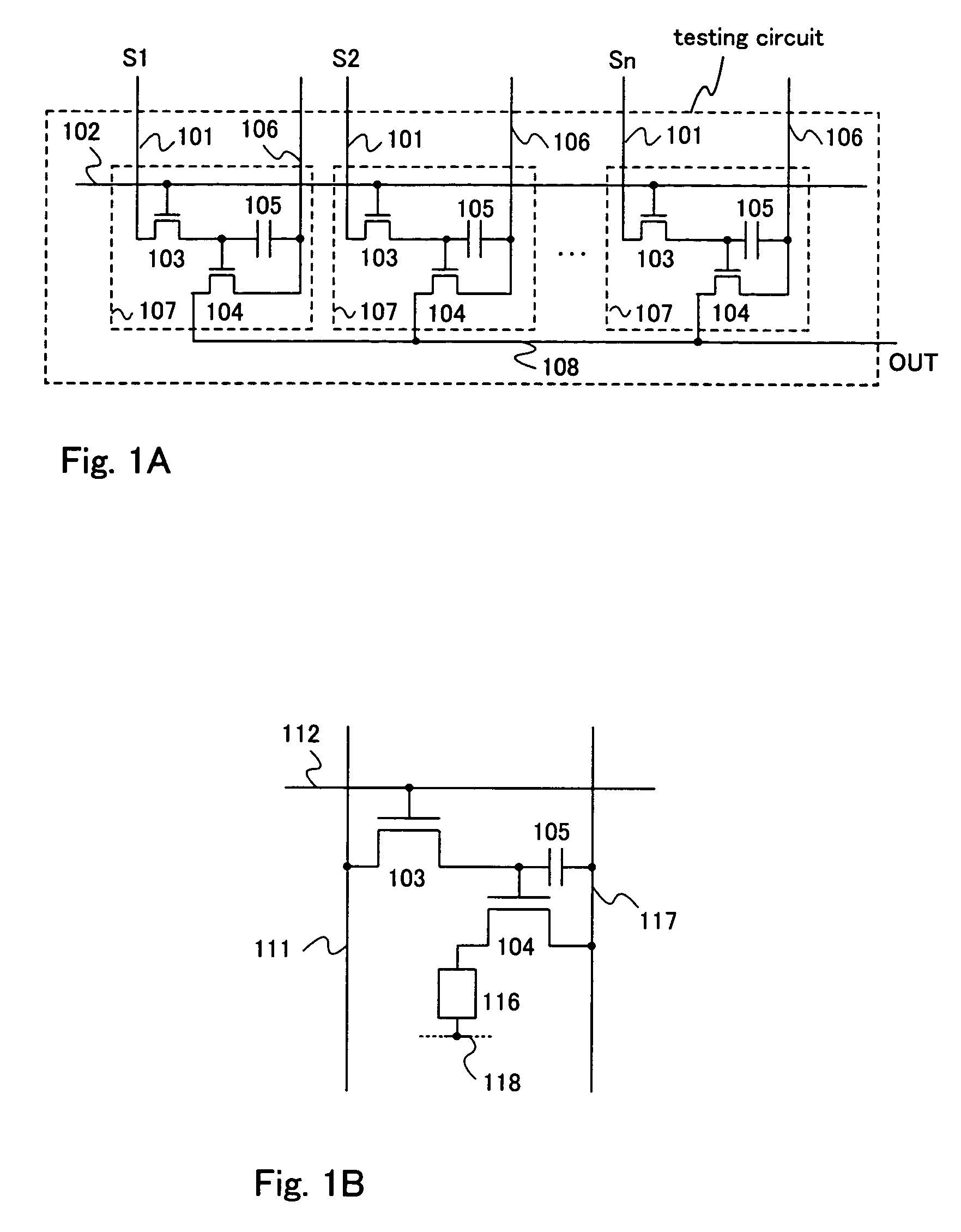
[0035]FIG. 1A shows a testing circuit according to the embodiment mode 1 of the invention. The testing circuit comprises a data signal line 101, a scanning line 102, a switching TFT 103, a driver TFT 104, a capacitor 105, a current supply line 106, a testing cell 107, and a testing line 108. The circuit of FIG. 1A is used for testing data signal lines. The testing circuit comprises a pixel circuit as shown in FIG. 1B and the testing cell 107 corresponds to the pixel circuit. The pixel circuit of FIG. 1B comprises a data signal line 111, a scanning line 112, a switching TFT 103, a driver TFT 104, a capacitor 105, an EL element 116, a current supply line 117, and a power source line 118.

[0036]In the pixel circuit, the driver TFT 104 supplies a current to the EL element 116 to emit light. The EL element 116 emits light in accordance with a potential of a video signal which is inputted to a gate of the driver TFT 104 from the source signal line 111 through the switching TFT 103.

[0037]Th...

embodiment mode 2

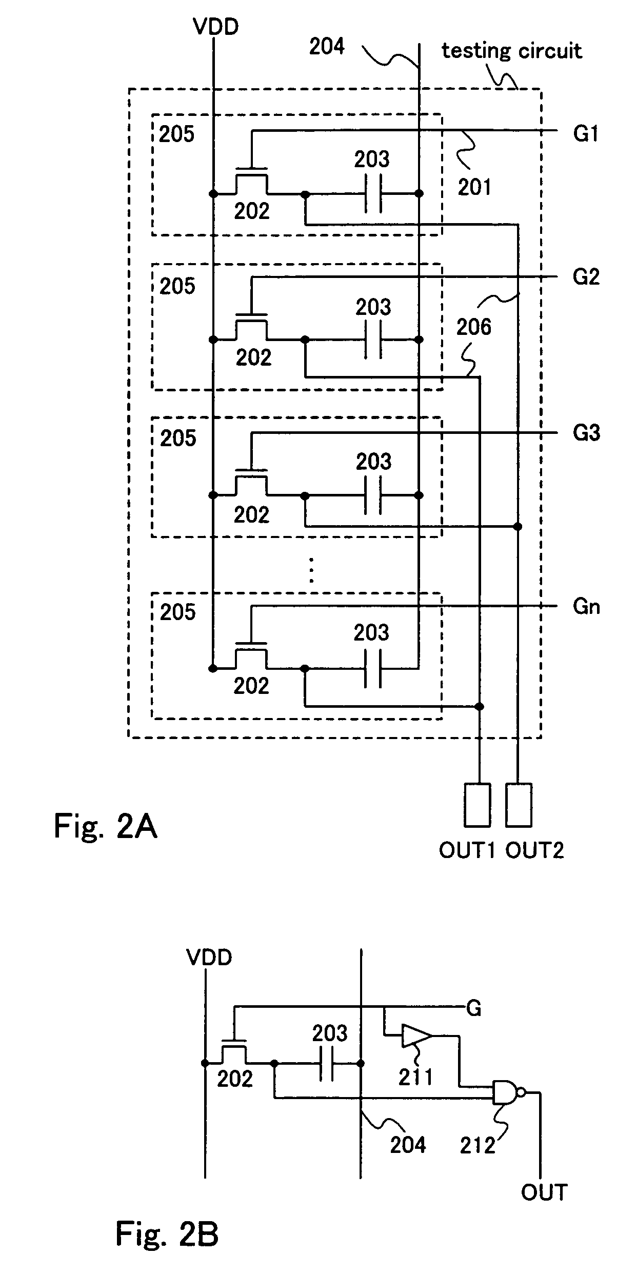
[0040]FIGS. 2A and 2B each shows a testing circuit according to the embodiment mode 2 of the invention. This circuit is used for the test of scanning lines. The testing circuit is prepared based on the pixel circuit of FIG. 1B as in embodiment mode 1, and a testing cell 205 in FIG. 2A corresponds to the pixel circuit.

[0041]The testing circuit in FIG. 2A comprises a scanning line 201, a switching TFT 202, a capacitor 203, a current supply line 204, a testing cell 205, and a testing line 206.

[0042]The configuration of the testing cell 205 is explained by comparison with a pixel circuit. An EL element and a driver TFT are removed from a pixel circuit. The power source line 118 connected to the EL element is detached from the drier TFT 104 and connected to the testing line 206. Also, the data signal line 111 shared by pixel circuits is detached from the source driver circuit and connected to the power voltage VDD, thereby the testing cell 205 is obtained. The switching TFT operates as a...

embodiment 1

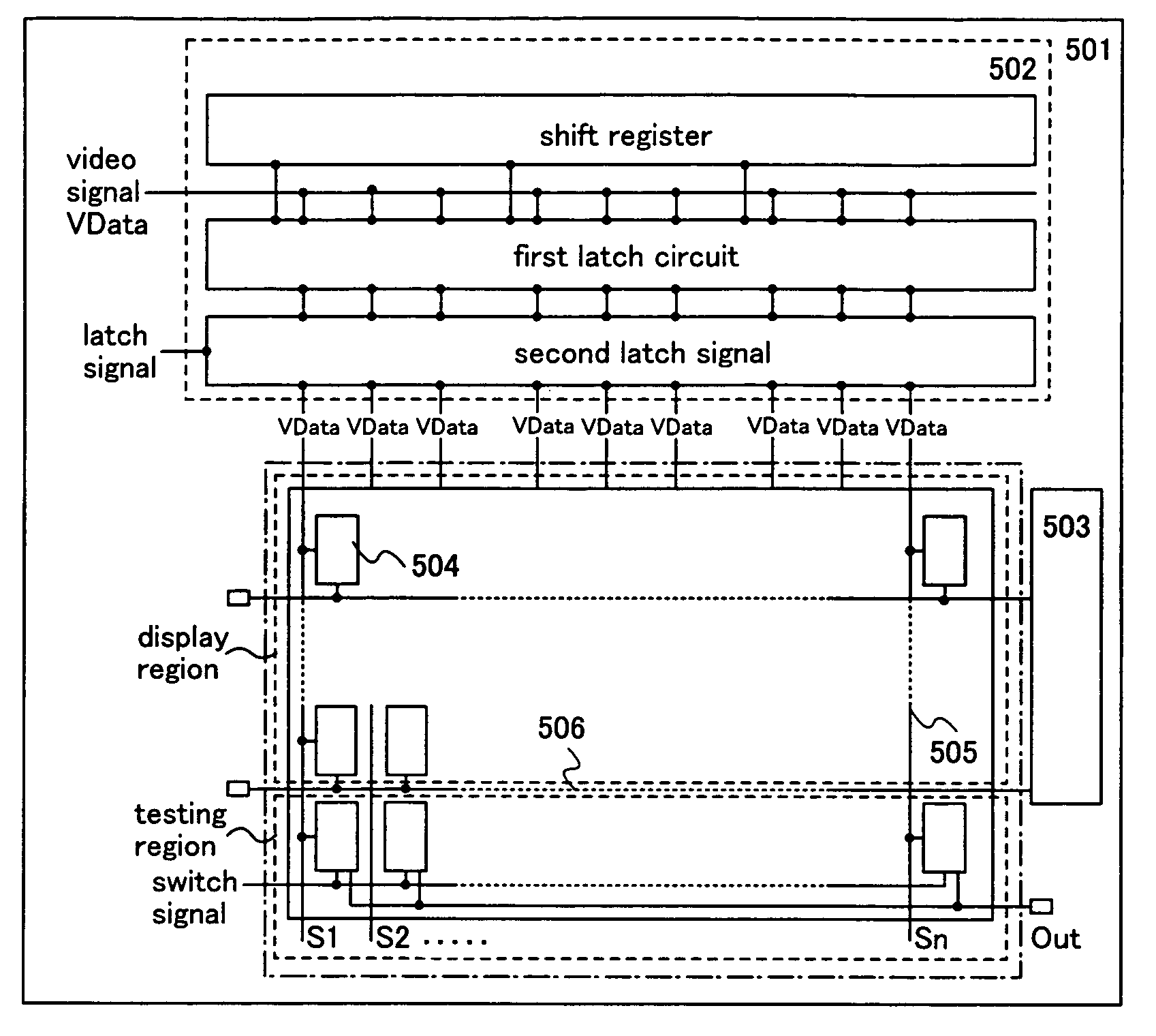
[0048]FIG. 5A shows embodiment 1 of the invention. A display device shown here comprises a substrate 501, a source driver circuit 502, a gate driver circuit 503, a pixel 504, a data signal line 505, and a scanning line 506. Among the pixels arranged in matrix, the last row of pixels opposed to the source driver circuit 502 is selected. In the case where dummy pixels are arranged in the periphery of a display region, they may be selected. The selected pixels are changed as follows. The EL element is removed from the pixel and the TFT in the pixel is detached from the power source line which is connected to the EL element, and connected to a testing terminal instead. One testing terminal is employed in the embodiment of FIG. 5A by connecting all the pixels in the row in common, although testing terminals may be plural if needed for the testing reason. Further, the scanning line 506 shared by pixels is detached from the gate driver circuit 503 so that an independent switch signal line ...


PUM


Abstract

It is the object of the present invention to provide a simple and accurate testing circuit and a testing method while occupying as small space as possible in an image display device. By partly changing dummy pixels arranged in the periphery of a display region into a testing circuit, tests for detecting broken wires in data signal lines and scanning lines and whether pixels are controlled adequately can be conducted easily and accurately, occupying as small space as possible without a need of an additional complicated circuit. Accordingly, a display panel can be produced at a low cost.

Description

BACKGROUND OF THE INVENTION[0001]1. Field of the Invention[0002]The present invention relates to an image display device in which a plurality of pixels are arranged in matrix and a method of testing the image display device.[0003]2. Description of the Related Art[0004]In recent years, image display devices such as a liquid crystal display (LCD), an electroluminescence (EL) display and the like have been advanced in precision and thus the degree of integration of elements has been remarkably improved as well.[0005]It is an essential part of the production line of image display device to test if a circuit mounted on a substrate operates normally before shipment as a finished panel. The test process itself has been becoming more complicated in accordance with the higher precision.[0006]FIG. 3 shows a configuration of a substrate on which a testing circuit is implemented in a conventional image display device. Such a configuration is shown, for example, in Japanese Patent Laid-Open No. ...

Claims


Application Information

Patent Timeline
IPC IPC(8): G01R31/00
CPCG09G3/006G09G3/32G09G2330/12G09G2300/08
Inventor OSADA, TAKESHI
Owner SEMICON ENERGY LAB CO LTD
Learn More