Silver under-layers for electroless cobalt alloys

a technology of silver underlayers and electroless cobalt, which is applied in the direction of liquid/solution decomposition chemical coating, semiconductor/solid-state device details, superimposed coating process, etc., can solve the problems of contaminating the dielectric material, and reducing the reliability of the overall circui

Active Publication Date: 2006-06-20
APPLIED MATERIALS INC
View PDF134 Cites 11 Cited by
  • Summary
  • Abstract
  • Description
  • Claims
  • Application Information

AI Technical Summary

Problems solved by technology

The use of copper as a conductive material poses several challenges.
Copper readily migrates under current and may contaminate the dielectric material by way of diffusion.
Copper oxides increase the resistance of the copper layer, become a source of particle contamination and reduce the reliability of the overall circuit.
However, copper does not easily catalyze or initiate the deposition of materials with lower reduction potential, such as cobalt or nickel, from conventional electroless solutions.
However, one difficulty of using a reducing current to initiate cobalt alloy deposition is the availability of a continuous conductive surface over the substrate surface.
A conductive surface may not be available with many applications, particularly after planarization of the copper and dielectric layers by chemical mechanical polishing (CMP) techniques.
However, deposition of the catalytic material may require multiple steps or use catalytic colloid compounds, such as palladium colloids.
Catalytic colloid compounds may adhere on dielectric materials and result in undesired, excessive and non-selective deposition of the cobalt alloy materials on the substrate surface.
Non-selective deposition of cobalt alloy materials may lead to surface contamination, unwanted diffusion of conductive materials into dielectric materials, and even device failure from short circuits and other device irregularities.
The higher resistivity reduces current and is not a desirable trait.
The deposition processes utilizing palladium or platinum are usually not efficient at plating or reducing the metal ions onto the copper surface and therefore much of the expensive and unconsumed metal ions are discarded as waste when the depleted deposition solution is discarded.
Furthermore, while platinum and palladium are often used as activation materials due to their high catalytic properties, platinum and palladium are often not easily deposited selectively on the conductive layer and contaminate the dielectric layer of a substrate surface.
Although cobalt alloys are deposited as capping layers to protect copper layers from destructive oxidation, cobalt alloys are susceptible to oxidation which forms metal alloyed oxides.
Metal oxides in the capping layer or on the copper layer are undesirable because of the increased resistivity.

Method used


Image

  • Silver under-layers for electroless cobalt alloys
  • Silver under-layers for electroless cobalt alloys
  • Silver under-layers for electroless cobalt alloys

Examples


Embodiment Construction

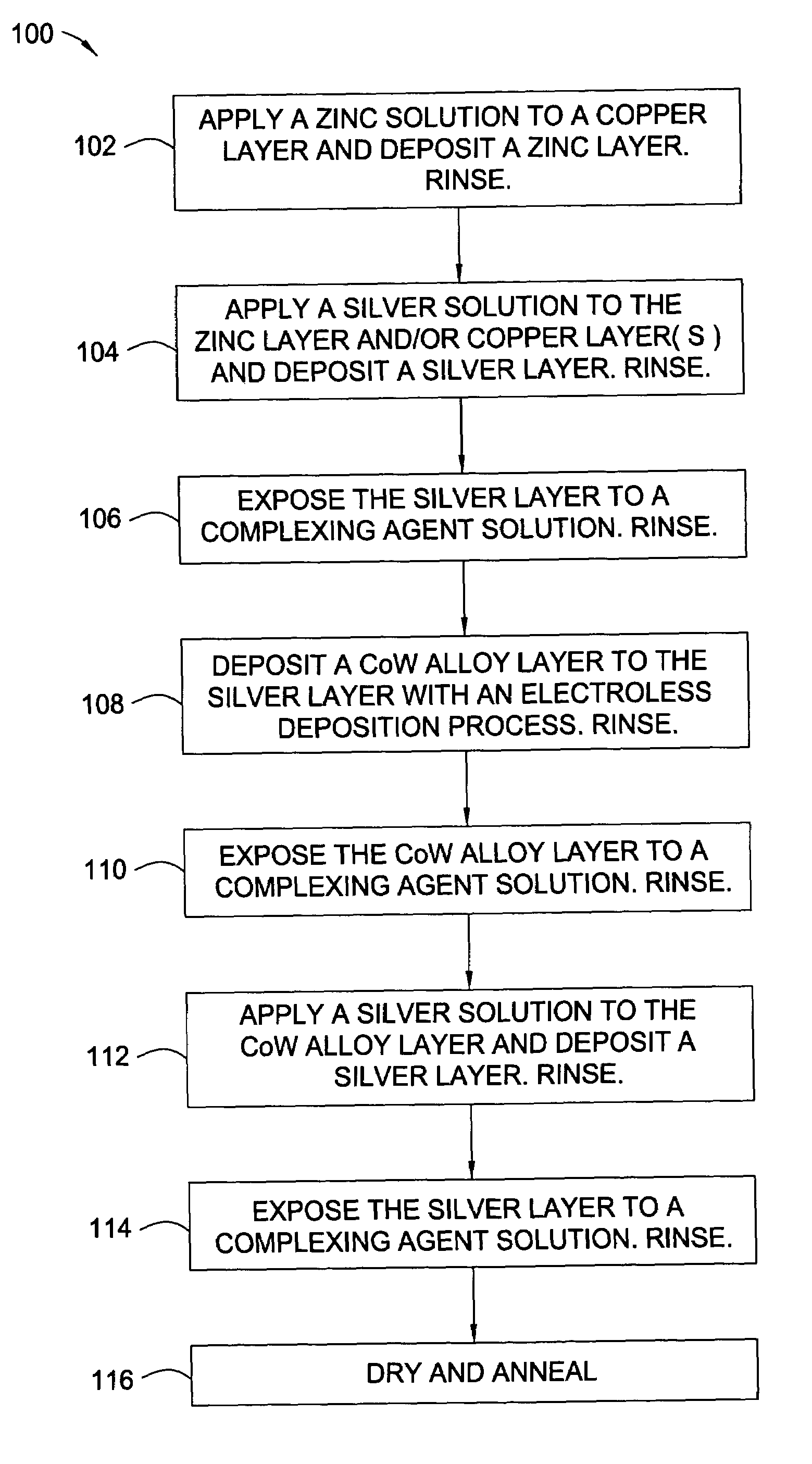
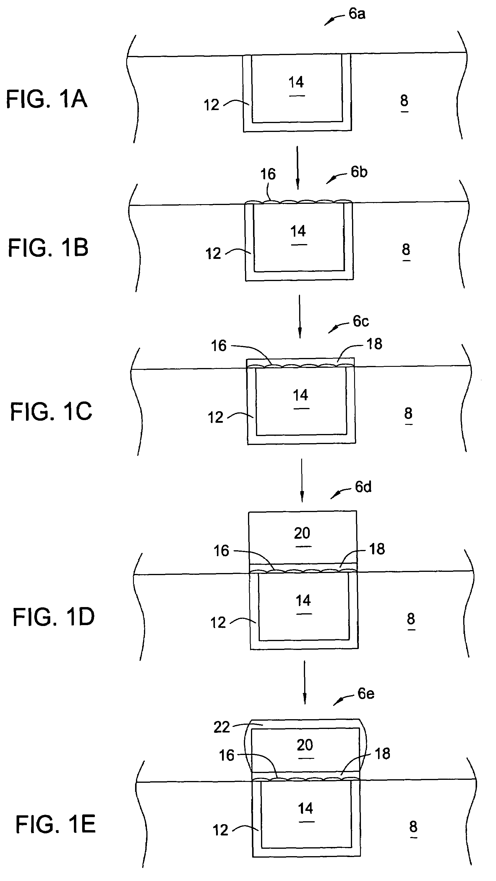
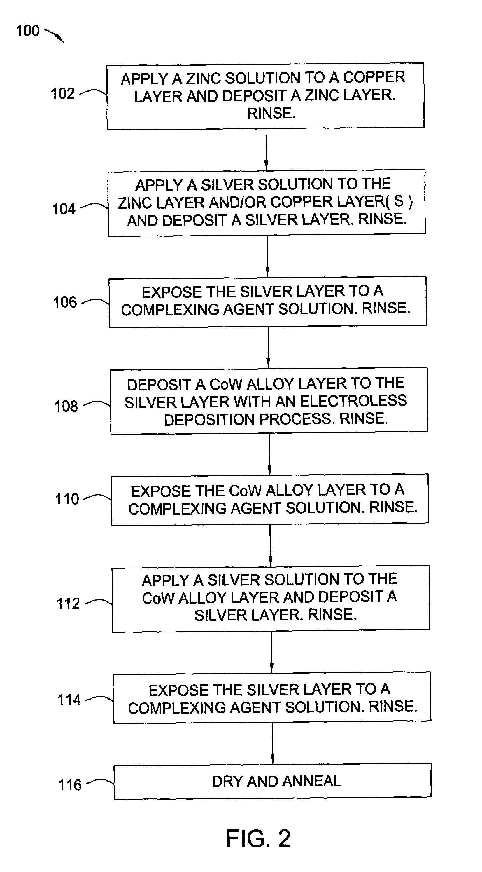
[0023]The words and phrases used herein should be given their ordinary and customary meaning in the art as understood by one skilled in the art unless otherwise further defined. Electroless deposition is broadly defined herein as deposition of a conductive material by a replacement reaction or exchange reaction wherein ions in a solution replace metal atoms in a surface while the metal atoms are ionized into the solution. Also, electroless deposition is broadly defined herein as deposition of a conductive material by ions in a bath over a catalytically active surface to deposit the conductive material by chemical reduction in the absence of an external electric current, such as in an autocatalytic reaction.

[0024]Embodiments of the invention include the deposition of a silver layer as an activation material to catalyze a subsequent deposition of a capping layer, such as a cobalt alloy layer. The catalytic properties of the activation material are characteristic of the coinage or nobl...


PUM

PropertyMeasurementUnit
concentrationaaaaaaaaaa

Abstract

In one embodiment, a method for depositing a capping layer on a substrate surface containing a copper layer is provided which includes exposing the substrate surface to a zinc solution, exposing the substrate surface to a silver solution to form a silver layer thereon and depositing the capping layer on the silver layer by an electroless deposition process. A second silver layer may be formed on the capping layer, if desired. In another embodiment, a composition of a deposition solution useful for forming a cobalt tungsten alloy contains calcium tungstate, a cobalt source at a concentration within a range from about 50 mM to about 500 mM, a complexing agent at a concentration within a range from about 100 mM to about 700 mM, and a buffering agent at a concentration within a range from about 50 mM to about 500 mM.

Description

CROSS-REFERENCE TO RELATED APPLICATIONS[0001]This application claims benefit of U.S. Provisional Patent Application Ser. No. 60 / 511,980, filed Oct. 15, 2003, which is herein incorporated by reference.BACKGROUND OF THE INVENTION[0002]1. Field of the Invention[0003]Embodiments of the invention generally relate to methods for activating a conductive material and depositing a capping layer on a semiconductor feature, and more particularly, at least in one embodiment, methods for depositing a silver activation layer on a copper surface for subsequent deposition of a cobalt alloy layer.[0004]2. Description of the Related Art[0005]Recent improvements in circuitry of ultra-large scale integration (ULSI) on substrates indicate that future generations of semiconductor devices will require smaller multi-level metallization with smaller geometric dimensions. The multilevel interconnects that lie at the heart of this technology require planarization of interconnect features formed in high aspect...

Claims


Application Information

Patent Timeline
Patent Type & Authority Patents(United States)
IPC IPC(8): H01L21/44C23C28/02C25D3/46C23C18/50H01L21/288H01L21/768H01L23/48H01L23/52H01L29/40
CPCC23C18/50C23C28/021C23C28/023H01L21/76874H01L21/76846H01L21/76849H01L21/76852H01L21/288
Inventor LOPATIN, SERGEY D.SHANMUGASUNDRUM, ARULKUMARSHACHAM-DIAMAND, YOSEF
Owner APPLIED MATERIALS INC
Why Eureka
Try Eureka