Contact Layers For Thin Film Solar Cells Employing Group IBIIIAVIA Compound Absorbers

a solar cell and compound absorber technology, applied in the direction of semiconductor/solid-state device manufacturing, electrical equipment, semiconductor devices, etc., can solve the problems of high cost of silicon-based solar cells, high cost of electricity generated by more traditional methods, and high cost of cylindrical targets, etc., to achieve high materials utilization and low cost

Inactive Publication Date: 2007-06-28
SOLOPOWER
View PDF39 Cites 52 Cited by
  • Summary
  • Abstract
  • Description
  • Claims
  • Application Information

AI Technical Summary

Problems solved by technology

However, the cost of electricity generated using silicon-based solar cells is higher than the cost of electricity generated by the more traditional methods.
Sputtering is an expensive vacuum technique with limited materials utilization.
Although cylindrical magnetron sputtering may increase this utilization to a higher range, cost involved in the preparation of a cylindrical target is higher than the cost of a planar target.

Method used


Image

  • Contact Layers For Thin Film Solar Cells Employing Group IBIIIAVIA Compound Absorbers
  • Contact Layers For Thin Film Solar Cells Employing Group IBIIIAVIA Compound Absorbers
  • Contact Layers For Thin Film Solar Cells Employing Group IBIIIAVIA Compound Absorbers

Examples


Embodiment Construction

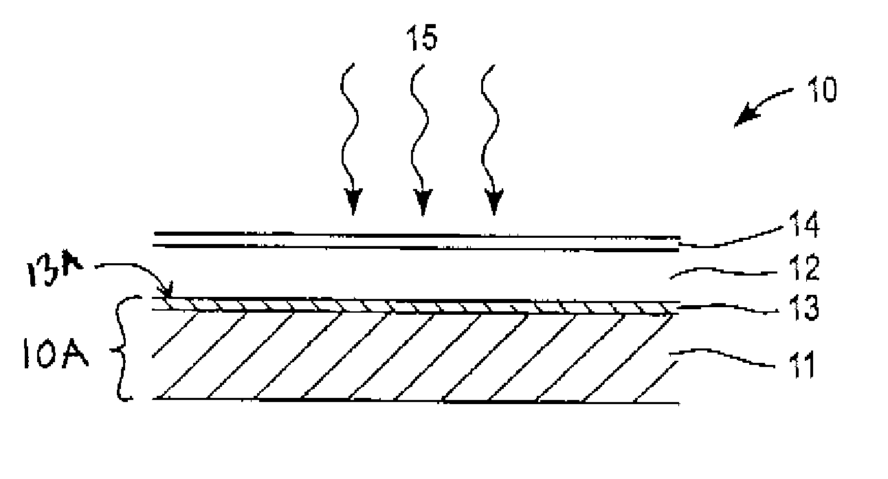
[0018] Present invention provides materials, methods and apparatus to fabricate conductive layers or contact layers for thin film solar cells, especially for those solar cells that employ Group IBIIIAVIA compound absorbers. Based on the brief review above one can conclude that irrespective of the specific approach employed in growing a CIGS(S) or Cu(In,Ga)(S,Se)2 type absorber film, the conductive layer 13 (or the contact layer) of FIG. 1 needs to have certain properties. These properties include, but are not limited to the following: i) the contact layer surface 13A should make a good ohmic contact to the absorber layer 12, ii) the contact layer 13 or the contact layer surface 13A should be stable in the reaction environments in which the absorber layer 12 is formed, i.e. they should not extensively react with Group VIA materials to the extent that they loose their ohmic nature or cause mechanical peeling problems, iii) the contact layer 13 or the contact layer surface 13A should n...


PUM


Abstract

The present invention provides methods and apparatus for deposition of contact layers for Group IBIIIAVIA solar cells using electrodeposition and / or electroless deposition approaches, and solar cells that result therefrom. In one aspect of the invention, the solar cell that results includes a substrate, a stacked contact layer that includes a bottom film coated on a surface of the substrate and a top film formed by electroplating over the bottom film, wherein the top film comprises at least one of Ru, Ir and Os. A Group IBIIIAVIA compound film formed over the top film. In another aspect of the invention, there is provided a method of depositing a stacked layer of a plurality of films in a plurality of sequentially disposed depositing units onto a continuously moving roll-to-roll sheet, preferably using electroplating of a stacked contact layer.

Description

CLAIM OF PRIORITY [0001] This application is a continuation-in-part of and claims priority to U.S. application Ser. No. 11 / 266,013 filed Nov. 2, 2005 entitled “Technique and Apparatus for Depositing Layers of Semiconductors for Solar Cell and Module Fabrication” and is a continuation in part of and claims priority to U.S. application Ser. No. 11 / 462,685 filed Aug. 4, 2006 entitled Technique for Preparing Precursor Films and Compound Layers for Thin Film Solar Cell Fabrication and Apparatus Corresponding Thereto”, and also claims priority to U.S. Provisional Appln. Ser. No. 60 / 862,164 filed Oct. 19, 2006 entitled “Roll-To-Roll Electroplating for Photovoltaic Film Manufacturing”, each of which are also expressly incorporated by reference herein.FIELD OF THE INVENTION [0002] The present invention relates to deposition of contact layers for Group IBIIIAVIA solar cells using electrodeposition and / or electroless deposition approaches. BACKGROUND [0003] Solar cells are photovoltaic devices...

Claims


Application Information

Patent Timeline
Patent Type & Authority Applications(United States)
IPC IPC(8): H01L31/00
CPCH01L31/022425H01L31/0322Y02E10/50H01L31/03923Y02E10/541
Inventor BASOL, BULENT M.
Owner SOLOPOWER
Why Eureka
Try Eureka