Apparatus and method for forming polycrystalline silicon thin film

a technology of polycrystalline silicon and polycrystalline silicon, applied in the direction of chemistry apparatus and processes, crystal growth processes, coatings, etc., can solve the problems of aforementioned pecvd limitation, the deposition process of the semiconductor device manufacturing process cannot be directly applied to the lcd manufacturing process, and the difference in the manufacturing process of lcd, so as to reduce the contamination, increase the crystallizing rate of amorphous silicon, and reduce the crystallizing temperature of amorphous silicon

Active Publication Date: 2007-03-08
WONIK IPS CO LTD
View PDF1 Cites 369 Cited by
  • Summary
  • Abstract
  • Description
  • Claims
  • Application Information

AI Technical Summary

Benefits of technology

[0047] An object of the present invention is to provide a method for forming a polycrystalline silicon thin film in which a metal layer having a distribution of metal particles suitable for forming a crystallization nucleus in an amorphous silicon layer, thus capable of increasing the crystallizing rate of an amorphous silicon, decreasing the crystallizing temperature of the amorphous silicon, and substantially decreasing a contamination due to the metal particles.
[0048] An object of the present invention is to provide a method for forming a polycrystalline silicon thin film in which metal nuclei are distributed at a low concentration, an ambient for suppressing a reaction of forming a metal silicide is prepared, a metal silicide having a extremely low concentration is formed on an amorphous silicon layer to enable the adjustment of the grain size, thus controlling the distribution concentration of the crystallization nuclei.
[0049] A further object of the present invention is to provide a method for forming a polycrystalline silicon thin film in which one cycle that metal nuclei can be distributed at a low concentration is performed, or the one cycle is divided into two or more cycles for a finer adjustment of the crystallization nuclei distribution.

Problems solved by technology

However, the LCD manufacturing process has a difference than the semiconductor device manufacturing process in that it uses a glass as a substrate instead of a wafer used in the semiconductor manufacturing process.
Therefore, the deposition process of the semiconductor device manufacturing process cannot be directly applied to the LCD manufacturing process.
However, the aforementioned PECVD has a limitation in that the silicon thin film formed is an amorphous silicon thin film.
In other words, since the amorphous silicon has a low electron mobility, it cannot be used in a circuit operating at a high speed.
The above-exemplified LCD increases a cost of the driving IC itself and its mounting cost.
Further, since an increase in resolution of the LCD panel requires a further decrease in pitch between pads for signal lines and scanning lines, it is difficult to perform a TCP bonding.
Resultantly, in view of trends toward a large-sized screen and a high picture quality of a flat panel display, the amorphous silicon TFT has a limitation in satisfying these requirements due to a low speed and a large volume.
However, in the distribution of the metal nuclei, the nickel target has a problem in that it is not suitable for a large-sized substrate.
However, since the nickel is a ferromagnetic material, it is difficult to form a magnetic field in an inside of the process space.
However, the method has a difficulty in preparing the target of which one side is 300 mm long using the present technique level.
Also, it is difficult to distribute a proper metal catalyst for a polycrystallinelization, which is due to an error that a thin film should be formed by a sputtering to perform the MILC process.
The sputtering for forming a thin film on an entire surface of the glass substrate for this purpose is an excessive process and apparatus in terms of the MILC process for the distribution of the crystallization nuclei.
In the polycrystalline thin film transistor by the MIC or MILC, it is confirmed that a large amount of metal diffused into the channel region is distributed to cause a serious metal contamination.
In other words, the contamination due to the metal impurity in the channel region has a large influence on the generation of a leakage current to deteriorate the field effect mobility and the threshold voltage characteristic and thus deteriorate the electrical property of the polysilicon thin film transistor.
In the long run, under a circumstance that a high temperature heat treatment is impossible due to the physical property of the glass substrate and a low temperature heat treatment must be inevitably performed, the forming of a metal catalyst layer for performing the low temperature heat treatment is inevitable.
However, by doing so, researchers face a dilemma that the supplied catalyst metal acts as a contamination material.
Meanwhile, it is a more important and basic problem that it is difficult to adjust the grain size in a preferred size range on the polysilicon thin film.
This means that the distribution concentration of metal particles as a catalyst for the adjustment of grain size cannot be adjusted by the sputtering or other thin film forming.
If the properties of the TFTs constituting the respective pixels are different, non-uniform picture quality is caused.
Thus, a large difference in the number of the grain boundaries in the channel regions of the same layer deteriorates the uniformity wholly.
However, the case shown in FIG. 1C secures the uniformity due to a very small grain size, but does not meet the characteristic requirements of the TFT.
Therefore, it is extremely natural that the sputtering fails to adjust the grain boundary.
In the related art MLIC, the addition of the crystallization nucleus allows a metal layer to be formed rather than allows the crystallization nucleus to be distributed into the amorphous silicon layer, so that it fails to provide means for forming a crystallization nucleus that can adjust the distribution concentration.

Method used


Image

  • Apparatus and method for forming polycrystalline silicon thin film
  • Apparatus and method for forming polycrystalline silicon thin film
  • Apparatus and method for forming polycrystalline silicon thin film

Examples


Embodiment Construction

[0065] The present invention will now be described more fully with reference to the accompanying drawings, in which exemplary embodiments of the invention are shown.

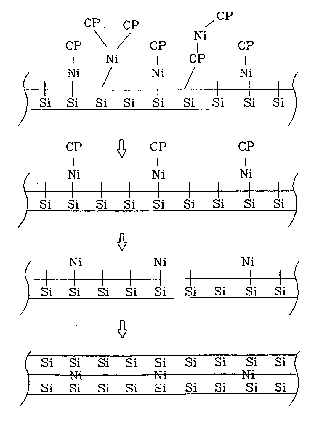
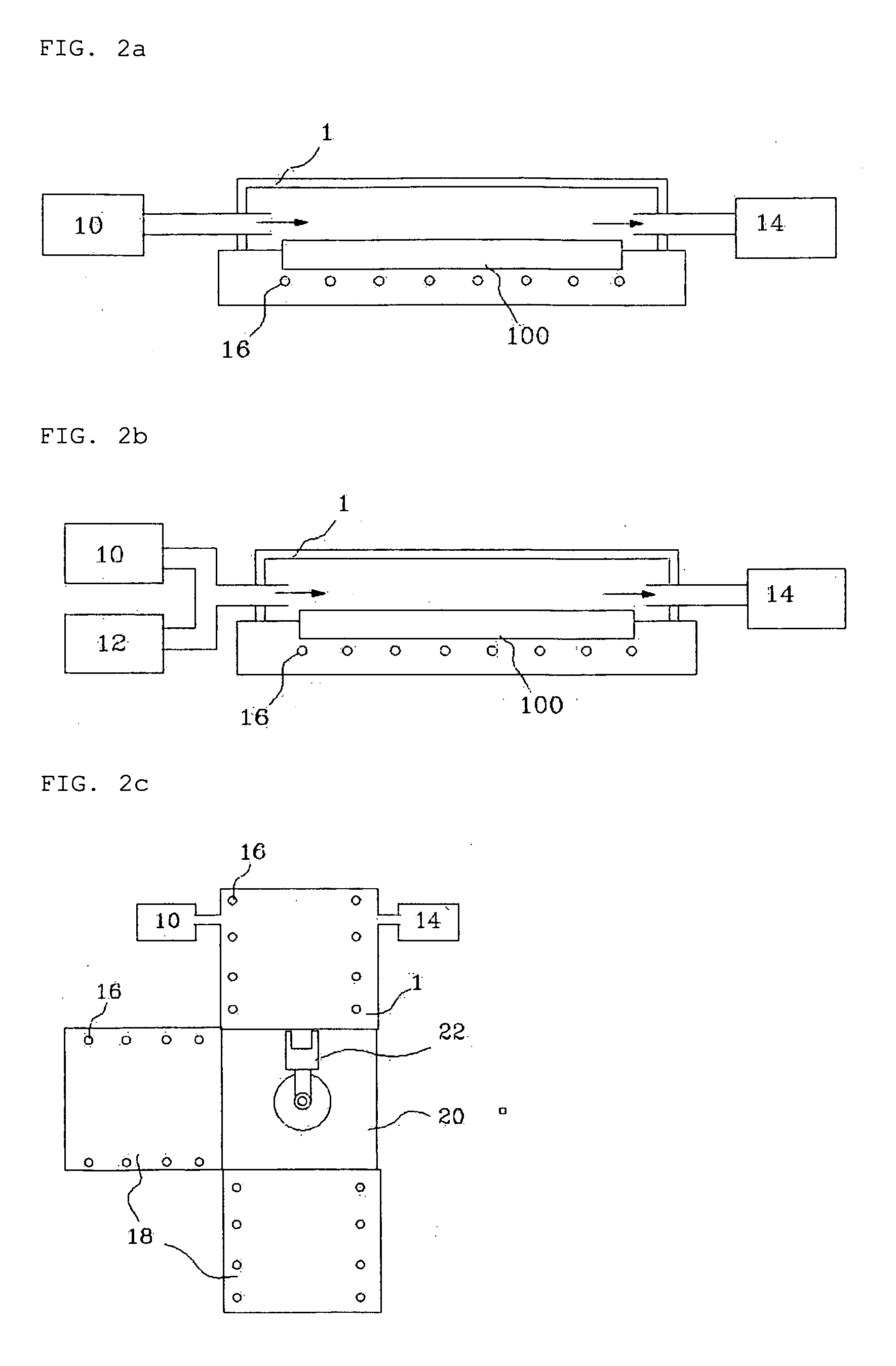
[0066]FIGS. 2A to 2C are concept views of atomic layer deposition (ALD) apparatuses designed to distribute a metal nucleus (Ni nucleus) as a catalyst on a glass substrate according to the present invention, FIG. 3 is a concept view showing that nickel molecules having a preoccupied region are adsorbed by Ni(C5H5)2 on an amorphous silicon, FIG. 4 is a side concept view illustrating steps that nickel nucleus as a metal nucleus according to the present invention is created, and FIGS. 5A to 5C are magnified photographs of polysilicon thin films illustrating that the grain size of the polysilicon thin films is adjusted according to an adjustment of distribution density of metal nuclei.

[0067] Also, FIG. 6 is a side concept view illustrating a step of adjusting a distribution density according to the present invention and FIG...


PUM

PropertyMeasurementUnit
temperatureaaaaaaaaaa
pressureaaaaaaaaaa
temperatureaaaaaaaaaa

Abstract

Apparatus and method for forming a polycrystalline silicon thin film by converting an amorphous silicon thin film into the polycrystalline silicon thin film using a metal are provided. The method includes: a metal nucleus adsorbing step of introducing a vapor phase metal compound into a process space where the glass substrate having the amorphous silicon formed thereon is disposed, to adsorb a metal nucleus contained in the metal compound into the amorphous silicon layer; a metal nucleus distribution region-forming step of forming a community region including a plurality of silicon particles every metal nucleus in a plane boundary region occupied by the metal compound by a self-limited mechanism due to the adsorption of the metal nucleus; and an excess gas removing step of purging and removing an excess gas which is not adsorbed in the metal nucleus distribution region-forming step.

Description

BACKGROUND OF THE INVENTION [0001] 1. Field of the Invention [0002] The present invention relates to apparatus and method for forming a polycrystalline silicon thin film from an amorphous silicon, using a metal. [0003] 2. Description of the Related Art [0004] Polycrystalline silicon (hereinafter referred to as ‘polysilicon) thin film employed in a technical field of the present invention is mainly used in a liquid crystal display (LCD), an organic electroluminescent (EL), or the like. [0005] For example, since the LCD does not have a self-luminescent property unlike the cathode ray tube (CRT), it needs a backlight but is widely used as one of flat panel displays due to advantages, such as a low power consumption, a portable lightweight and slim profile and the like. [0006] The LCD uses a color filter to display colors. A unit pixel of the color filter is comprised of R, G and B sub-pixels. The LCD employs a matrix control way to display colors through these respective pixels. [0007]...

Claims


Application Information

Patent Timeline
Patent Type & Authority Applications(United States)
IPC IPC(8): H01L21/31
CPCC23C16/18C23C16/24C23C16/45525C23C16/45555Y10T117/1016H01L21/02422H01L21/02532H01L21/02672C23C16/56
Inventor JANG, TAEK YONGLEE, BYOUNG ILLEE, YOUNG HO
Owner WONIK IPS CO LTD
Why Eureka
Try Eureka