Method for crystallizing amorphous silicon and fabricating thin film transistor using crystallized silicon

a technology of amorphous silicon and crystallization method, which is applied in the direction of transistors, semiconductor devices, electrical devices, etc., can solve the problems of lowering the breakdown voltage of the device, high liquid crystal display cost, and high cost of driving circuit, etc., and achieves the effect of enhancing the crystallization ra

Inactive Publication Date: 2002-07-04
LG DISPLAY CO LTD
View PDF0 Cites 19 Cited by
  • Summary
  • Abstract
  • Description
  • Claims
  • Application Information

AI Technical Summary

Benefits of technology

[0023] Another object of the present invention is to provide a method for crystallizing an amorphous silicon layer by enhancing a crystallization rate.
[0024] Another object of the present invention is to provide a method for crystallizing an amorphous silicon layer at a relatively low temperature.

Problems solved by technology

The driving circuit, however, is very expensive, and thus the liquid crystal display including the large scale integration costs also high.
The solid phase crystallization (SPC) method, however, results in an irregular grain growth and irregular grain boundaries so that the gate insulating layer on the polycrystalline silicon layer grows erratically, thereby lowering breakdown voltage of the device.
In addition, since the grain sizes of the polycrystalline silicon are excessively non-uniform, electrical characteristics, such as current and a threshold voltage, are not good.
Further, a costly quartz substrate should be employed.
However, use of this method has been limited by the lack of control over some of the process steps.
Since it is difficult to precisely control the laser, the multiple shots introduce non-uniformities into the annealing process.
TFTs made by this method are significantly more expensive than those made by direct deposition or SPC.
However, there are some problems in the conventional field enhanced metal induced crystallization (FEMIC) method.
The residual metal catalyst causes a deterioration of the polycrystalline silicon layer.
Furthermore, during the crystallization processes, heat loss occurs in the entire surface of the amorphous silicon layer.

Method used


Image

  • Method for crystallizing amorphous silicon and fabricating thin film transistor using crystallized silicon
  • Method for crystallizing amorphous silicon and fabricating thin film transistor using crystallized silicon
  • Method for crystallizing amorphous silicon and fabricating thin film transistor using crystallized silicon

Examples


Embodiment Construction

[0040] Reference will now be made in detail to the illustrated embodiments of the present invention, examples of which are illustrated in the accompanying drawings. Wherever possible, the same reference numbers will be used throughout the drawings to refer to the same or like parts.

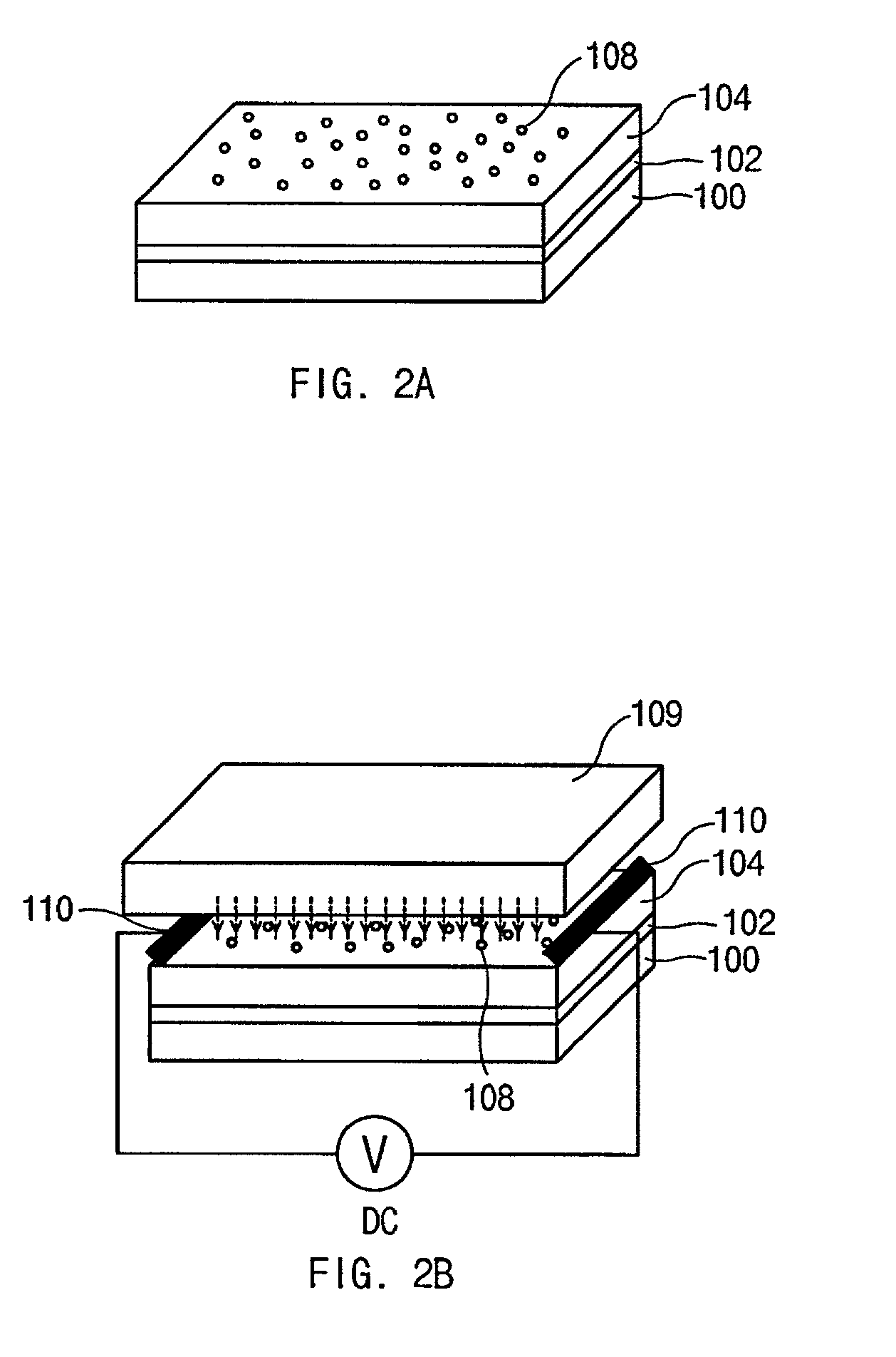
[0041] FIGS. 2A to 2D are perspective views showing crystallization steps of an amorphous silicon layer according to a first embodiment of the present invention.

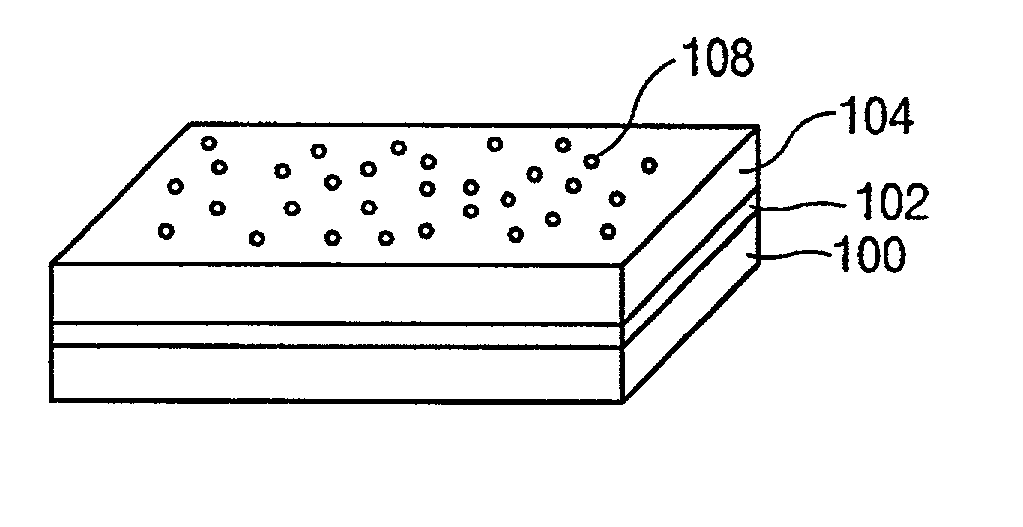
[0042] Referring to FIG. 2A, a buffer layer 102 is formed on a substrate 100, and then an amorphous silicon layer 104 is formed on the buffer layer 102. The buffer layer 102 on the substrate 100 prevents an impurity diffusion from the substrate 100 into the amorphous silicon layer 104. In this present invention, silicon oxide (SiO.sub.2) may be selected as the buffer layer 102. Thereafter, a very small amount of catalytic metal clusters 108, such as nickel (Ni), is deposited on the entire surface of the amorphous silicon layer 104 by using evapora...


PUM

PropertyMeasurementUnit
electric fieldaaaaaaaaaa
lattice constantaaaaaaaaaa

Abstract

A method of crystallizing amorphous silicon includes forming an amorphous silicon layer over a substrate, forming a plurality of metal clusters on the amorphous silicon layer, and simultaneously applying a thermal treatment, an electric field, and a magnetic field to crystallize the amorphous silicon layer.

Description

[0001] This application claims the benefit of Korean Application No. P2000-86333 filed on Dec. 29, 2000, which is hereby incorporated by reference.BACKGROUND OF THE INVENTION[0002] 1. Field of the Invention[0003] The present invention relates to a method for crystallizing amorphous silicon, and more particularly, to method for crystallizing amorphous silicon and fabricating a thin film transistor using the crystallized silicon.[0004] 2. Discussion of the Related Art[0005] Due to a rapid development in information technologies, display devices are developed in accordance with the pace of the technology development. Display devices process and display a great deal of information. A cathode ray tube (CRT) has served as a mainstream of the display devices. To meet the needs of the current technology break-through, a flat panel display device having small size, light weight, and low power consumption is a more important area in research.[0006] In general, liquid crystal display (LCD) dev...

Claims


Application Information

Patent Timeline
Patent Type & Authority Applications(United States)
IPC IPC(8): H01L21/20H01L21/336H01L21/77H01L21/84H01L27/12H01L29/786
CPCH01L21/2022H01L29/66757H01L29/78675H01L27/1277H01L27/1285H01L21/02488H01L21/02422H01L21/02532H01L21/02672H01L29/786
Inventor KIM, HAE-YEOLKIMKIM, SE-JUNE
Owner LG DISPLAY CO LTD
Why Eureka
Try Eureka