Interconnect with low dielectric constant insulators for semiconductor integrated circuit manufacturing

a technology of dielectric constant insulator and integrated circuit, which is applied in the direction of semiconductor/solid-state device manufacturing, basic electric elements, electric apparatus, etc., can solve the problems of affecting the performance and reliability of the fabricated circuit, the use of low-k materials as ild in the interconnect is not mature, and the embedded low-k dielectric integration process suffers

Inactive Publication Date: 2001-02-13
NEWPORT FAB
View PDF13 Cites 355 Cited by
  • Summary
  • Abstract
  • Description
  • Claims
  • Application Information

AI Technical Summary

Problems solved by technology

The quality of the interconnect structure drastically affects the performance and reliability of the fabricated circuit.
However, the use of low-k materials as ILD in the interconnect is not mature at this time, and processes still need to be developed for accommodating the low-k material when forming the interconnect.
Unfortunately, these embedded low-k dielectric integration processes suffer from the following disadvantages.
For example, ensuring that the level of the low-k material is the same as the top surfaces of the metal or interconnect lines is difficult for at least four reasons.
First, in practical manufacturing, it is impossible to deposit a film of low-k material at a precise film thickness from wafer to wafer.
Second, even within a wafer, depositing an absolutely uniform low-k film across the same wafer is not possible, since the typical thickness non-uniformity of the low-k film deposited by either spin-on coating or chemical vapor deposition (CVD) using currently-available technology varies by about one to ten percent.
Third, even within a given die on a wafer, the gaps between the metal lines are of different sizes, leading to uneven film height of the low-k material above the metal lines.
Fourth, removing low-k film to the precise thickness during the etch-back is impossible to control in manufacturing.
This difficulty of controlling the deposition and etch-back of the low-k material so that the surface level of the low-k material is the same as the top surfaces of all the metal or interconnect lines results in the following two problems: (1) insufficient-etch-back of the low-k material, which results in a poisoned via and problems associated therewith, and (2) excessive-etch-back of the low-k material, which results in the increase in inter-metal line capacitance and problems associated therewith.
Consequently, applying the correct etch-back amount for the low-k material with the required tolerance (hereinafter referred to as a "process window") is difficult for these proposed processes that embed low-k materials.
Missing the process window, for whatever reason, results in poor interconnect integrity and reliability, or degradation in interconnect performance.
However, as explained above, the etch-back of the low-k material 3, which is critical for this isolation to occur, is difficult to control.
The poisoned vias 8 present a serious yield and reliability problem in the conventional embedded low-k interconnect structures.
A discontinuous liner leads to poor metal growth and a poor connection.
Furthermore, the higher inter-line capacitance increases cross-talk noise, which is the unwanted transfer of signals from one metal line to another metal line.
Even if the process window is met for some metal lines, other metal lines may miss the process window.
For example, the metal lines that are spaced further apart from each other experience excessive-etch-back of the low-k material (i.e., the level of the low-k material in these gaps are lower than the height of the metal lines) because the increased spacings between these metal lines.
In summary, missing the process window leads to either poor interconnect integrity and reliability or degradation in performance of the circuits.
Furthermore, it is very difficult or impossible to embed the low-k materials precisely in the metal gaps of different sizes by the low-k film deposition and the etch-back process.
Consequently, the improvement to the overall integrated circuit performance that is provided by the incorporation of low-k material is limited.
As noted earlier, poisoned vias 8a lead to poor plug formation that results in poor contact between the metal layers.
However, increasing the metal area causes several disadvantages.
First, an increased metal area causes an increased pitch, thereby reducing interconnect density per layer.
Adding additional layers of interconnects increases the costs to manufacture the wafer and can also lead to lower yields.
Second, even after the metal area has been increased, special care is still required to ensure that the wafers are processed within the misalignment tolerance provided by the increased metal area.

Method used


Image

  • Interconnect with low dielectric constant insulators for semiconductor integrated circuit manufacturing
  • Interconnect with low dielectric constant insulators for semiconductor integrated circuit manufacturing
  • Interconnect with low dielectric constant insulators for semiconductor integrated circuit manufacturing

Examples


first embodiment

G A LOW-K ETCH-BACK STEP (PERFECTLY ALIGNED VIAS)

FIGS. 4A-4E are vertical cross-sectional views that illustrate selected stages of fabrication of the interconnect structure according to the first embodiment of the present invention where perfect alignment between via and metal line can be obtained. Referring to FIG. 4A, a substrate 14p is provided. Substrate 14p may, for example, include transistors, diodes, and other integrated circuit elements (not shown). A first metal layer 10p is deposited over substrate 14p. Metal layer 10p can include electrically conducting material, such as aluminum, titanium, or titanium-nitride, although other conductive material can be employed. Sacrificial layer 18p is deposited on first metal layer 10p. Sacrificial layer 18p includes a height that is used to increase the process window for low-k material 26p etch-back as described previously.

First metal layer 10p and sacrificial layer 18p are patterned to form metal lines each having a sacrificial laye...

second embodiment

LOW-K POLISH STEP INSTEAD OF LOW-K ETCH-BACK STEP

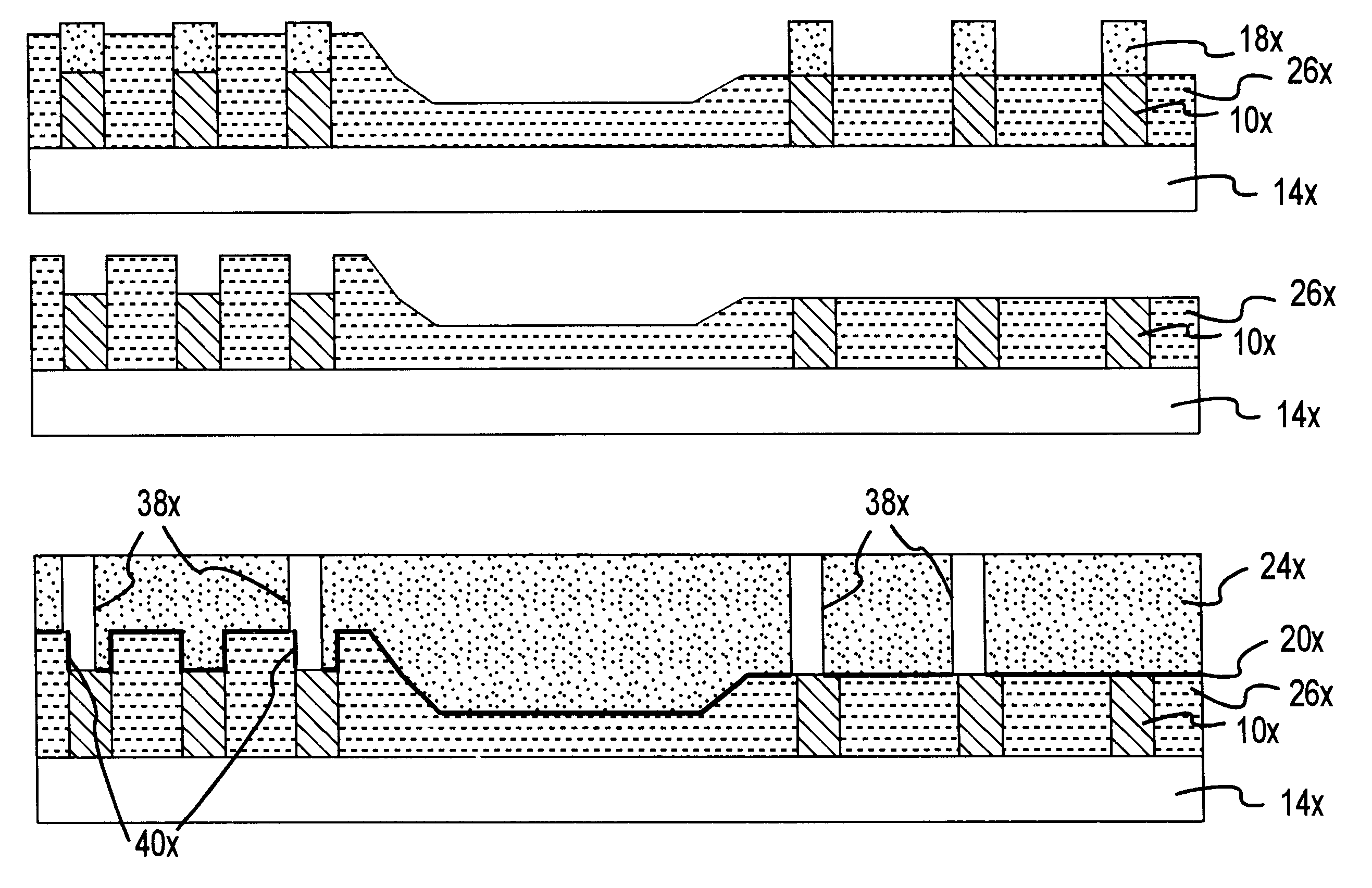
FIGS. 5A-5I are vertical cross-sectional views that illustrate selected stages of fabrication of the interconnect structure according to a second embodiment of the present invention. FIG. 5A is a vertical cross-sectional view of the interconnect structure after the processing steps illustrated in FIGS. 3A-3E (i.e., after metal layer 10y and sacrificial layer 18y have been deposited on substrate 14y and patterned, and low-k material 26y has been deposited to fill gaps between metal lines 10y and to cover sacrificial layer 18y). Referring back to FIG. 5B, low-k material 26y is removed by a chemical mechanical polish (CMP) process step.

For the sake of brevity, since FIGS. 5C-5I correspond generally to FIGS. 3G-3M, the description of FIGS. 3G-3M, 7A, and 7B as they relate to FIGS. 5C-5I will not be repeated herein. Instead, it is noted that the interconnect structure differs from that of the second embodiment in the following ways: (1) lo...

third embodiment

G BOTH A LOW-K PLANARIZATION STEP AND A LOW-K ETCH-BACK STEP

FIGS. 6A-6D are vertical cross-sectional views that illustrate selected stages of fabrication of the interconnect structure according to a third embodiment of the present invention. FIG. 6A is a vertical cross-sectional view of the interconnect structure after the processing steps illustrated in FIGS. 3A-3E, (i.e., after metal layer 10z and sacrificial layer 18z have been deposited on substrate 14z and patterned, and low-k material 26z has been deposited to cover substrate 14z and gap fill metal layer 10z and sacrificial layer 18z). Referring to FIG. 6B, low-k material 26z is removed by a CMP process step to a level that is higher than the sacrificial layer 18z. Referring to FIG. 6C, low-k material 26z is further removed by an etch-back process, such as by plasma etch. Referring to FIG. 6D, sacrificial layer 18z is then removed.

The processing steps in this embodiment that occur after FIG. 6D correspond generally to FIGS. 3H...


PUM

PropertyMeasurementUnit
thicknessaaaaaaaaaa
thicknessaaaaaaaaaa
thicknessaaaaaaaaaa

Abstract

A method is provided for forming an improved interconnect structure on a semiconductor body. A first metal layer is deposited on the semiconductor body. A sacrificial layer having a height is deposited on the first metal layer. The sacrificial layer and the metal layer are patterned to form separate metal lines with the sacrificial layer remaining on said metal lines. A low-k material is then deposited to fill the gaps between metal lines and to cover the sacrificial layer. The low-k material is then removed to a level within the height of the sacrificial layer. The sacrificial layer is then removed. A protective layer is deposited on top of the metal lines and the low-k material. A dielectric layer is deposited over the protective layer. The protective layer protects the low-k material from attack by chemicals utilized by subsequent process steps to etch vias in the dielectric layer, to strip photo-resist, and to clean the vias. The protective layer is then selectively etched away to make contact between a via plug and the metal lines.

Description

1. Field of the InventionThis invention relates generally to semiconductor processing, and more specifically to multi-level interconnects with low dielectric constant insulators and methods for fabricating the same.2. Background ArtModern integrated circuits are made up of literally millions of active and passive devices such as transistors, capacitors, and resistors. These devices are initially isolated from one another but are later connected together to form functional circuits through interconnect structures. The quality of the interconnect structure drastically affects the performance and reliability of the fabricated circuit. Interconnects are increasingly determining the limits of performance and density of modern ultra large scale integrated (ULSI) circuits.Conventional interconnect structures employ one or more metal layers. Each metal layer is typically made from aluminum alloys or tungsten. Interlevel and intralevel dielectrics (ILDs), such as silicon dioxide (SiO.sub.2),...

Claims


Application Information

Patent Timeline
Patent Type & Authority Patents(United States)
IPC IPC(8): H01L21/70H01L21/768
CPCH01L21/76801H01L21/76802H01L21/76819H01L21/76834
Inventor ZHAO, BINBRONGO, MAUREEN R.
Owner NEWPORT FAB
Why Eureka
Try Eureka